{"title":"功率mosfet的栅极电荷控制开关波形设计","authors":"Hirotaka Oomori, Ichiro Omura","doi":"10.1016/j.pedc.2022.100018","DOIUrl":null,"url":null,"abstract":"<div><p>The switching waveform design, especially controlling and optimizing the slew rate, is an efficient technique to mitigate the trade-off between decreasing the loss and increasing the noise of the switching power device. The digital active gate driver which generates the gate waveform to achieve the designed switching waveform requires a significant computational burden because the optimum driving point is searched automatically and comprehensively. This paper proposes a novel and simple method to calculate gate waveforms to achieve the designed switching waveforms. This method calculates how much gate charge is additionally required to match the designed waveform by exploiting the voltage and current response of the power device to the small gate charge pulse. The validation of this method is demonstrated by simulation in the case of both the drain-source voltage design and the drain current design. The deviation from the designed waveform is quantified in this paper.</p></div>","PeriodicalId":74483,"journal":{"name":"Power electronic devices and components","volume":"3 ","pages":"Article 100018"},"PeriodicalIF":0.0000,"publicationDate":"2022-10-01","publicationTypes":"Journal Article","fieldsOfStudy":null,"isOpenAccess":false,"openAccessPdf":"https://www.sciencedirect.com/science/article/pii/S2772370422000153/pdfft?md5=b83dd185ca87b3991d4b9846e79cd436&pid=1-s2.0-S2772370422000153-main.pdf","citationCount":"1","resultStr":"{\"title\":\"Switching waveform design with gate charge control for power MOSFETs\",\"authors\":\"Hirotaka Oomori, Ichiro Omura\",\"doi\":\"10.1016/j.pedc.2022.100018\",\"DOIUrl\":null,\"url\":null,\"abstract\":\"<div><p>The switching waveform design, especially controlling and optimizing the slew rate, is an efficient technique to mitigate the trade-off between decreasing the loss and increasing the noise of the switching power device. The digital active gate driver which generates the gate waveform to achieve the designed switching waveform requires a significant computational burden because the optimum driving point is searched automatically and comprehensively. This paper proposes a novel and simple method to calculate gate waveforms to achieve the designed switching waveforms. This method calculates how much gate charge is additionally required to match the designed waveform by exploiting the voltage and current response of the power device to the small gate charge pulse. The validation of this method is demonstrated by simulation in the case of both the drain-source voltage design and the drain current design. The deviation from the designed waveform is quantified in this paper.</p></div>\",\"PeriodicalId\":74483,\"journal\":{\"name\":\"Power electronic devices and components\",\"volume\":\"3 \",\"pages\":\"Article 100018\"},\"PeriodicalIF\":0.0000,\"publicationDate\":\"2022-10-01\",\"publicationTypes\":\"Journal Article\",\"fieldsOfStudy\":null,\"isOpenAccess\":false,\"openAccessPdf\":\"https://www.sciencedirect.com/science/article/pii/S2772370422000153/pdfft?md5=b83dd185ca87b3991d4b9846e79cd436&pid=1-s2.0-S2772370422000153-main.pdf\",\"citationCount\":\"1\",\"resultStr\":null,\"platform\":\"Semanticscholar\",\"paperid\":null,\"PeriodicalName\":\"Power electronic devices and components\",\"FirstCategoryId\":\"1085\",\"ListUrlMain\":\"https://www.sciencedirect.com/science/article/pii/S2772370422000153\",\"RegionNum\":0,\"RegionCategory\":null,\"ArticlePicture\":[],\"TitleCN\":null,\"AbstractTextCN\":null,\"PMCID\":null,\"EPubDate\":\"\",\"PubModel\":\"\",\"JCR\":\"\",\"JCRName\":\"\",\"Score\":null,\"Total\":0}","platform":"Semanticscholar","paperid":null,"PeriodicalName":"Power electronic devices and components","FirstCategoryId":"1085","ListUrlMain":"https://www.sciencedirect.com/science/article/pii/S2772370422000153","RegionNum":0,"RegionCategory":null,"ArticlePicture":[],"TitleCN":null,"AbstractTextCN":null,"PMCID":null,"EPubDate":"","PubModel":"","JCR":"","JCRName":"","Score":null,"Total":0}
Switching waveform design with gate charge control for power MOSFETs
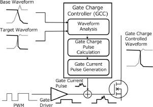
The switching waveform design, especially controlling and optimizing the slew rate, is an efficient technique to mitigate the trade-off between decreasing the loss and increasing the noise of the switching power device. The digital active gate driver which generates the gate waveform to achieve the designed switching waveform requires a significant computational burden because the optimum driving point is searched automatically and comprehensively. This paper proposes a novel and simple method to calculate gate waveforms to achieve the designed switching waveforms. This method calculates how much gate charge is additionally required to match the designed waveform by exploiting the voltage and current response of the power device to the small gate charge pulse. The validation of this method is demonstrated by simulation in the case of both the drain-source voltage design and the drain current design. The deviation from the designed waveform is quantified in this paper.
Power electronic devices and componentsHardware and Architecture, Electrical and Electronic Engineering, Atomic and Molecular Physics, and Optics, Safety, Risk, Reliability and Quality

 求助内容:
求助内容: 应助结果提醒方式:


