Kaiyue He, Jijie Zhu, Zishun Li, Zhe Chen, Hehe Zhang, Chao Liu, Xu Zhang, Shuo Wang, Peiyi Zhao, Yu Zhou, Shizheng Zhang, Yao Yin, Xiaorui Zheng, Wei Huang, Lin Wang
{"title":"超短通道高灵敏度二维PbI2光电探测器","authors":"Kaiyue He, Jijie Zhu, Zishun Li, Zhe Chen, Hehe Zhang, Chao Liu, Xu Zhang, Shuo Wang, Peiyi Zhao, Yu Zhou, Shizheng Zhang, Yao Yin, Xiaorui Zheng, Wei Huang, Lin Wang","doi":"10.1007/s11467-023-1323-1","DOIUrl":null,"url":null,"abstract":"<div><p>Photodetectors based on two-dimensional (2D) semiconductors have attracted many research interests owing to their excellent optoelectronic characteristics and application potential for highly integrated applications. However, the unique morphology of 2D materials also restricts the further improvement of the device performance, as the carrier transport is very susceptible to intrinsic and extrinsic environment of the materials. Here, we report the highest responsivity (172 A/W) achieved so far for a PbI<sub>2</sub>-based photodetector at room temperature, which is an order of magnitude higher than previously reported. Thermal scanning probe lithography (t-SPL) was used to pattern electrodes to realize the ultrashort channel (~60 nm) in the device. The shortening of the channel length greatly reduces the probability of the photo-generated carriers being scattered during the transport process, which increases the photocurrent density and thus the responsivity. Our work shows that the combination of emerging processing technologies and 2D materials is an effective route to shrink device size and improve device performance.\n</p><div><figure><div><div><picture><source><img></source></picture></div></div></figure></div></div>","PeriodicalId":573,"journal":{"name":"Frontiers of Physics","volume":"18 6","pages":""},"PeriodicalIF":6.5000,"publicationDate":"2023-07-26","publicationTypes":"Journal Article","fieldsOfStudy":null,"isOpenAccess":false,"openAccessPdf":"","citationCount":"0","resultStr":"{\"title\":\"High-sensitive two-dimensional PbI2 photodetector with ultrashort channel\",\"authors\":\"Kaiyue He, Jijie Zhu, Zishun Li, Zhe Chen, Hehe Zhang, Chao Liu, Xu Zhang, Shuo Wang, Peiyi Zhao, Yu Zhou, Shizheng Zhang, Yao Yin, Xiaorui Zheng, Wei Huang, Lin Wang\",\"doi\":\"10.1007/s11467-023-1323-1\",\"DOIUrl\":null,\"url\":null,\"abstract\":\"<div><p>Photodetectors based on two-dimensional (2D) semiconductors have attracted many research interests owing to their excellent optoelectronic characteristics and application potential for highly integrated applications. However, the unique morphology of 2D materials also restricts the further improvement of the device performance, as the carrier transport is very susceptible to intrinsic and extrinsic environment of the materials. Here, we report the highest responsivity (172 A/W) achieved so far for a PbI<sub>2</sub>-based photodetector at room temperature, which is an order of magnitude higher than previously reported. Thermal scanning probe lithography (t-SPL) was used to pattern electrodes to realize the ultrashort channel (~60 nm) in the device. The shortening of the channel length greatly reduces the probability of the photo-generated carriers being scattered during the transport process, which increases the photocurrent density and thus the responsivity. Our work shows that the combination of emerging processing technologies and 2D materials is an effective route to shrink device size and improve device performance.\\n</p><div><figure><div><div><picture><source><img></source></picture></div></div></figure></div></div>\",\"PeriodicalId\":573,\"journal\":{\"name\":\"Frontiers of Physics\",\"volume\":\"18 6\",\"pages\":\"\"},\"PeriodicalIF\":6.5000,\"publicationDate\":\"2023-07-26\",\"publicationTypes\":\"Journal Article\",\"fieldsOfStudy\":null,\"isOpenAccess\":false,\"openAccessPdf\":\"\",\"citationCount\":\"0\",\"resultStr\":null,\"platform\":\"Semanticscholar\",\"paperid\":null,\"PeriodicalName\":\"Frontiers of Physics\",\"FirstCategoryId\":\"101\",\"ListUrlMain\":\"https://link.springer.com/article/10.1007/s11467-023-1323-1\",\"RegionNum\":2,\"RegionCategory\":\"物理与天体物理\",\"ArticlePicture\":[],\"TitleCN\":null,\"AbstractTextCN\":null,\"PMCID\":null,\"EPubDate\":\"\",\"PubModel\":\"\",\"JCR\":\"Q1\",\"JCRName\":\"PHYSICS, MULTIDISCIPLINARY\",\"Score\":null,\"Total\":0}","platform":"Semanticscholar","paperid":null,"PeriodicalName":"Frontiers of Physics","FirstCategoryId":"101","ListUrlMain":"https://link.springer.com/article/10.1007/s11467-023-1323-1","RegionNum":2,"RegionCategory":"物理与天体物理","ArticlePicture":[],"TitleCN":null,"AbstractTextCN":null,"PMCID":null,"EPubDate":"","PubModel":"","JCR":"Q1","JCRName":"PHYSICS, MULTIDISCIPLINARY","Score":null,"Total":0}
High-sensitive two-dimensional PbI2 photodetector with ultrashort channel
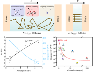
Photodetectors based on two-dimensional (2D) semiconductors have attracted many research interests owing to their excellent optoelectronic characteristics and application potential for highly integrated applications. However, the unique morphology of 2D materials also restricts the further improvement of the device performance, as the carrier transport is very susceptible to intrinsic and extrinsic environment of the materials. Here, we report the highest responsivity (172 A/W) achieved so far for a PbI2-based photodetector at room temperature, which is an order of magnitude higher than previously reported. Thermal scanning probe lithography (t-SPL) was used to pattern electrodes to realize the ultrashort channel (~60 nm) in the device. The shortening of the channel length greatly reduces the probability of the photo-generated carriers being scattered during the transport process, which increases the photocurrent density and thus the responsivity. Our work shows that the combination of emerging processing technologies and 2D materials is an effective route to shrink device size and improve device performance.
期刊介绍:
Frontiers of Physics is an international peer-reviewed journal dedicated to showcasing the latest advancements and significant progress in various research areas within the field of physics. The journal's scope is broad, covering a range of topics that include:
Quantum computation and quantum information
Atomic, molecular, and optical physics
Condensed matter physics, material sciences, and interdisciplinary research
Particle, nuclear physics, astrophysics, and cosmology
The journal's mission is to highlight frontier achievements, hot topics, and cross-disciplinary points in physics, facilitating communication and idea exchange among physicists both in China and internationally. It serves as a platform for researchers to share their findings and insights, fostering collaboration and innovation across different areas of physics.
 求助内容:
求助内容: 应助结果提醒方式:


