Gihyeon Kwon, Yoon-Ho Choi, Hyangsook Lee, Hyeon-Sik Kim, Jeahun Jeong, Kwangsik Jeong, Min Baik, Hoedon Kwon, Jaemin Ahn, Eunha Lee, Mann-Ho Cho
{"title":"
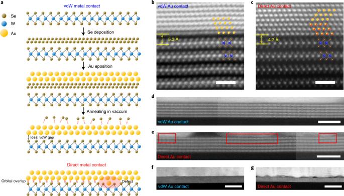
金属与二维半导体之间无相互作用和无缺陷的范德华接触","authors":"Gihyeon Kwon, Yoon-Ho Choi, Hyangsook Lee, Hyeon-Sik Kim, Jeahun Jeong, Kwangsik Jeong, Min Baik, Hoedon Kwon, Jaemin Ahn, Eunha Lee, Mann-Ho Cho","doi":"10.1038/s41928-022-00746-6","DOIUrl":null,"url":null,"abstract":"High Schottky barrier heights at metal–semiconductor junctions due to Fermi-level pinning can degrade the performance of electronic devices and increase their energy consumption. Van der Waals contacts between metals and two-dimensional semiconductors without Fermi-level pinning are theoretically possible, but have not been achieved due to the presence of interactions such as interface defects and orbital overlap. Here we show that interaction- and defect-free van der Waals contacts can be formed between a range of metals and two-dimensional semiconductors via a metal deposition process that uses a selenium buffer layer. Our contacts obey the Schottky–Mott rule and have a Fermi-level pinning of –0.91. A comparison between the van der Waals contacts and typical direct metal contacts reveals differences in interface gap distances, band bending and electrical characteristics. Using gold van der Waals contacts, we fabricate p-type tungsten diselenide field-effect transistors that exhibit stable operation with on/off ratio of 106, mobility of 155 cm2 (V s)–1, contact resistance of 1.25 kΩ μm and Schottky barrier height of 60 meV. High-quality van der Waals contacts between metals and two-dimensional semiconductors can be created using a selenium buffer layer that is deposited before the metal deposition process.","PeriodicalId":19064,"journal":{"name":"Nature Electronics","volume":"5 4","pages":"241-247"},"PeriodicalIF":40.9000,"publicationDate":"2022-04-21","publicationTypes":"Journal Article","fieldsOfStudy":null,"isOpenAccess":false,"openAccessPdf":"","citationCount":"45","resultStr":"{\"title\":\"Interaction- and defect-free van der Waals contacts between metals and two-dimensional semiconductors\",\"authors\":\"Gihyeon Kwon, Yoon-Ho Choi, Hyangsook Lee, Hyeon-Sik Kim, Jeahun Jeong, Kwangsik Jeong, Min Baik, Hoedon Kwon, Jaemin Ahn, Eunha Lee, Mann-Ho Cho\",\"doi\":\"10.1038/s41928-022-00746-6\",\"DOIUrl\":null,\"url\":null,\"abstract\":\"High Schottky barrier heights at metal–semiconductor junctions due to Fermi-level pinning can degrade the performance of electronic devices and increase their energy consumption. Van der Waals contacts between metals and two-dimensional semiconductors without Fermi-level pinning are theoretically possible, but have not been achieved due to the presence of interactions such as interface defects and orbital overlap. Here we show that interaction- and defect-free van der Waals contacts can be formed between a range of metals and two-dimensional semiconductors via a metal deposition process that uses a selenium buffer layer. Our contacts obey the Schottky–Mott rule and have a Fermi-level pinning of –0.91. A comparison between the van der Waals contacts and typical direct metal contacts reveals differences in interface gap distances, band bending and electrical characteristics. Using gold van der Waals contacts, we fabricate p-type tungsten diselenide field-effect transistors that exhibit stable operation with on/off ratio of 106, mobility of 155 cm2 (V s)–1, contact resistance of 1.25 kΩ μm and Schottky barrier height of 60 meV. High-quality van der Waals contacts between metals and two-dimensional semiconductors can be created using a selenium buffer layer that is deposited before the metal deposition process.\",\"PeriodicalId\":19064,\"journal\":{\"name\":\"Nature Electronics\",\"volume\":\"5 4\",\"pages\":\"241-247\"},\"PeriodicalIF\":40.9000,\"publicationDate\":\"2022-04-21\",\"publicationTypes\":\"Journal Article\",\"fieldsOfStudy\":null,\"isOpenAccess\":false,\"openAccessPdf\":\"\",\"citationCount\":\"45\",\"resultStr\":null,\"platform\":\"Semanticscholar\",\"paperid\":null,\"PeriodicalName\":\"Nature Electronics\",\"FirstCategoryId\":\"5\",\"ListUrlMain\":\"https://www.nature.com/articles/s41928-022-00746-6\",\"RegionNum\":1,\"RegionCategory\":\"工程技术\",\"ArticlePicture\":[],\"TitleCN\":null,\"AbstractTextCN\":null,\"PMCID\":null,\"EPubDate\":\"\",\"PubModel\":\"\",\"JCR\":\"Q1\",\"JCRName\":\"ENGINEERING, ELECTRICAL & ELECTRONIC\",\"Score\":null,\"Total\":0}","platform":"Semanticscholar","paperid":null,"PeriodicalName":"Nature Electronics","FirstCategoryId":"5","ListUrlMain":"https://www.nature.com/articles/s41928-022-00746-6","RegionNum":1,"RegionCategory":"工程技术","ArticlePicture":[],"TitleCN":null,"AbstractTextCN":null,"PMCID":null,"EPubDate":"","PubModel":"","JCR":"Q1","JCRName":"ENGINEERING, ELECTRICAL & ELECTRONIC","Score":null,"Total":0}
引用次数: 45
摘要
费米级引脚导致金属半导体结的肖特基势垒高度过高,会降低电子设备的性能并增加其能耗。金属与二维半导体之间不存在费米级钉销的范德华接触理论上是可行的,但由于存在界面缺陷和轨道重叠等相互作用,尚未实现。在这里,我们展示了通过使用硒缓冲层的金属沉积工艺,可以在一系列金属和二维半导体之间形成无相互作用和无缺陷的范德华接触。我们的接触符合肖特基-莫特规则,费米级引脚为-0.91。通过比较范德华触点和典型的直接金属触点,可以发现两者在界面间隙距离、带弯曲和电气特性方面存在差异。我们利用金范德华触点制造出了 p 型二硒化钨场效应晶体管,这些晶体管工作稳定,导通/关断比为 106,迁移率为 155 cm2 (V s)-1,接触电阻为 1.25 kΩ μm,肖特基势垒高度为 60 meV。利用在金属沉积过程之前沉积的硒缓冲层,可以在金属和二维半导体之间建立高质量的范德华接触。
Interaction- and defect-free van der Waals contacts between metals and two-dimensional semiconductors
High Schottky barrier heights at metal–semiconductor junctions due to Fermi-level pinning can degrade the performance of electronic devices and increase their energy consumption. Van der Waals contacts between metals and two-dimensional semiconductors without Fermi-level pinning are theoretically possible, but have not been achieved due to the presence of interactions such as interface defects and orbital overlap. Here we show that interaction- and defect-free van der Waals contacts can be formed between a range of metals and two-dimensional semiconductors via a metal deposition process that uses a selenium buffer layer. Our contacts obey the Schottky–Mott rule and have a Fermi-level pinning of –0.91. A comparison between the van der Waals contacts and typical direct metal contacts reveals differences in interface gap distances, band bending and electrical characteristics. Using gold van der Waals contacts, we fabricate p-type tungsten diselenide field-effect transistors that exhibit stable operation with on/off ratio of 106, mobility of 155 cm2 (V s)–1, contact resistance of 1.25 kΩ μm and Schottky barrier height of 60 meV. High-quality van der Waals contacts between metals and two-dimensional semiconductors can be created using a selenium buffer layer that is deposited before the metal deposition process.
期刊介绍:
Nature Electronics is a comprehensive journal that publishes both fundamental and applied research in the field of electronics. It encompasses a wide range of topics, including the study of new phenomena and devices, the design and construction of electronic circuits, and the practical applications of electronics. In addition, the journal explores the commercial and industrial aspects of electronics research.
The primary focus of Nature Electronics is on the development of technology and its potential impact on society. The journal incorporates the contributions of scientists, engineers, and industry professionals, offering a platform for their research findings. Moreover, Nature Electronics provides insightful commentary, thorough reviews, and analysis of the key issues that shape the field, as well as the technologies that are reshaping society.
Like all journals within the prestigious Nature brand, Nature Electronics upholds the highest standards of quality. It maintains a dedicated team of professional editors and follows a fair and rigorous peer-review process. The journal also ensures impeccable copy-editing and production, enabling swift publication. Additionally, Nature Electronics prides itself on its editorial independence, ensuring unbiased and impartial reporting.
In summary, Nature Electronics is a leading journal that publishes cutting-edge research in electronics. With its multidisciplinary approach and commitment to excellence, the journal serves as a valuable resource for scientists, engineers, and industry professionals seeking to stay at the forefront of advancements in the field.