光电压场效应晶体管

IF 50.5 1区 综合性期刊 Q1 MULTIDISCIPLINARY SCIENCES
Nature Pub Date : 2017-02-08 DOI:10.1038/nature21050
Valerio Adinolfi, Edward H. Sargent
{"title":"光电压场效应晶体管","authors":"Valerio Adinolfi, Edward H. Sargent","doi":"10.1038/nature21050","DOIUrl":null,"url":null,"abstract":"A photovoltage field-effect transistor is demonstrated that is very sensitive to infrared light and has high gain. Silicon is the workhorse of modern electronic devices, but it performs poorly as a platform for photodetection in the infrared. Valerio Adinolfi and Edward Sargent offer a solution to this shortcoming in the form of a new device architecture, something they call the ''photovoltage field-effect transistor''. The idea is not to try to manipulate the light sensitivity of the silicon itself, but instead to use infrared-sensitive quantum dots as the main photo-responsive element. The absorbed light generates a photovoltage in the quantum-dot layer, which is in turn used to modulate the electronic response of the underlying silicon transistor. The result is a silicon-based infrared photodetector whose performance compares well with state-of-the-art devices based on more complex and costly semiconducting systems. The detection of infrared radiation enables night vision, health monitoring, optical communications and three-dimensional object recognition. Silicon is widely used in modern electronics, but its electronic bandgap prevents the detection of light at wavelengths longer than about 1,100 nanometres. It is therefore of interest to extend the performance of silicon photodetectors into the infrared spectrum, beyond the bandgap of silicon1,2. Here we demonstrate a photovoltage field-effect transistor that uses silicon for charge transport, but is also sensitive to infrared light owing to the use of a quantum dot light absorber. The photovoltage generated at the interface between the silicon and the quantum dot, combined with the high transconductance provided by the silicon device, leads to high gain (more than 104 electrons per photon at 1,500 nanometres), fast time response (less than 10 microseconds) and a widely tunable spectral response. Our photovoltage field-effect transistor has a responsivity that is five orders of magnitude higher at a wavelength of 1,500 nanometres than that of previous infrared-sensitized silicon detectors3. The sensitization is achieved using a room-temperature solution process and does not rely on traditional high-temperature epitaxial growth of semiconductors (such as is used for germanium and III–V semiconductors)4,5. Our results show that colloidal quantum dots can be used as an efficient platform for silicon-based infrared detection, competitive with state-of-the-art epitaxial semiconductors.","PeriodicalId":18787,"journal":{"name":"Nature","volume":"542 7641","pages":"324-327"},"PeriodicalIF":50.5000,"publicationDate":"2017-02-08","publicationTypes":"Journal Article","fieldsOfStudy":null,"isOpenAccess":false,"openAccessPdf":"https://sci-hub-pdf.com/10.1038/nature21050","citationCount":"168","resultStr":"{\"title\":\"Photovoltage field-effect transistors\",\"authors\":\"Valerio Adinolfi, Edward H. Sargent\",\"doi\":\"10.1038/nature21050\",\"DOIUrl\":null,\"url\":null,\"abstract\":\"A photovoltage field-effect transistor is demonstrated that is very sensitive to infrared light and has high gain. Silicon is the workhorse of modern electronic devices, but it performs poorly as a platform for photodetection in the infrared. Valerio Adinolfi and Edward Sargent offer a solution to this shortcoming in the form of a new device architecture, something they call the ''photovoltage field-effect transistor''. The idea is not to try to manipulate the light sensitivity of the silicon itself, but instead to use infrared-sensitive quantum dots as the main photo-responsive element. The absorbed light generates a photovoltage in the quantum-dot layer, which is in turn used to modulate the electronic response of the underlying silicon transistor. The result is a silicon-based infrared photodetector whose performance compares well with state-of-the-art devices based on more complex and costly semiconducting systems. The detection of infrared radiation enables night vision, health monitoring, optical communications and three-dimensional object recognition. Silicon is widely used in modern electronics, but its electronic bandgap prevents the detection of light at wavelengths longer than about 1,100 nanometres. It is therefore of interest to extend the performance of silicon photodetectors into the infrared spectrum, beyond the bandgap of silicon1,2. Here we demonstrate a photovoltage field-effect transistor that uses silicon for charge transport, but is also sensitive to infrared light owing to the use of a quantum dot light absorber. The photovoltage generated at the interface between the silicon and the quantum dot, combined with the high transconductance provided by the silicon device, leads to high gain (more than 104 electrons per photon at 1,500 nanometres), fast time response (less than 10 microseconds) and a widely tunable spectral response. Our photovoltage field-effect transistor has a responsivity that is five orders of magnitude higher at a wavelength of 1,500 nanometres than that of previous infrared-sensitized silicon detectors3. The sensitization is achieved using a room-temperature solution process and does not rely on traditional high-temperature epitaxial growth of semiconductors (such as is used for germanium and III–V semiconductors)4,5. Our results show that colloidal quantum dots can be used as an efficient platform for silicon-based infrared detection, competitive with state-of-the-art epitaxial semiconductors.\",\"PeriodicalId\":18787,\"journal\":{\"name\":\"Nature\",\"volume\":\"542 7641\",\"pages\":\"324-327\"},\"PeriodicalIF\":50.5000,\"publicationDate\":\"2017-02-08\",\"publicationTypes\":\"Journal Article\",\"fieldsOfStudy\":null,\"isOpenAccess\":false,\"openAccessPdf\":\"https://sci-hub-pdf.com/10.1038/nature21050\",\"citationCount\":\"168\",\"resultStr\":null,\"platform\":\"Semanticscholar\",\"paperid\":null,\"PeriodicalName\":\"Nature\",\"FirstCategoryId\":\"103\",\"ListUrlMain\":\"https://www.nature.com/articles/nature21050\",\"RegionNum\":1,\"RegionCategory\":\"综合性期刊\",\"ArticlePicture\":[],\"TitleCN\":null,\"AbstractTextCN\":null,\"PMCID\":null,\"EPubDate\":\"\",\"PubModel\":\"\",\"JCR\":\"Q1\",\"JCRName\":\"MULTIDISCIPLINARY SCIENCES\",\"Score\":null,\"Total\":0}","platform":"Semanticscholar","paperid":null,"PeriodicalName":"Nature","FirstCategoryId":"103","ListUrlMain":"https://www.nature.com/articles/nature21050","RegionNum":1,"RegionCategory":"综合性期刊","ArticlePicture":[],"TitleCN":null,"AbstractTextCN":null,"PMCID":null,"EPubDate":"","PubModel":"","JCR":"Q1","JCRName":"MULTIDISCIPLINARY SCIENCES","Score":null,"Total":0}
引用次数: 168

摘要

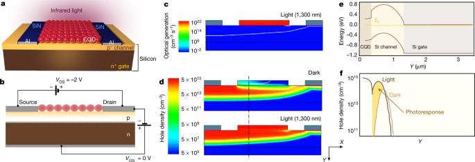
展示了一种对红外光非常敏感且具有高增益的光电压场效应晶体管。硅是现代电子设备的主力,但作为红外光探测平台,它的性能却很差。瓦莱里奥-阿迪诺尔菲和爱德华-萨金特针对这一缺陷提出了一种新器件结构的解决方案,他们称之为 "光电压场效应晶体管"。他们的想法不是试图操纵硅本身的光敏性,而是使用对红外线敏感的量子点作为主要的光反应元件。被吸收的光在量子点层中产生光电压,反过来又用来调节底层硅晶体管的电子响应。这种硅基红外线光电探测器的性能可与基于更复杂、更昂贵的半导体系统的先进设备媲美。红外辐射检测可用于夜视、健康监测、光通信和三维物体识别。硅被广泛应用于现代电子产品中,但其电子带隙阻碍了对波长超过约 1,100 纳米的光的探测。因此,将硅光电探测器的性能扩展到硅带隙以外的红外光谱是很有意义的1,2。在这里,我们展示了一种光电压场效应晶体管,它使用硅进行电荷传输,但由于使用了量子点光吸收器,因此对红外光也很敏感。在硅和量子点之间的界面上产生的光电压与硅器件提供的高跨导相结合,产生了高增益(在 1,500 纳米处每光子超过 104 个电子)、快速时间响应(小于 10 微秒)和广泛的可调光谱响应。在波长为 1,500 纳米时,我们的光电压场效应晶体管的响应速度比以前的红外敏化硅探测器高五个数量级3。敏化是通过室温溶液工艺实现的,并不依赖于传统的半导体高温外延生长(如用于锗和 III-V 半导体的外延生长)4,5。我们的研究结果表明,胶体量子点可用作硅基红外探测的高效平台,与最先进的外延半导体相比具有竞争力。
本文章由计算机程序翻译,如有差异,请以英文原文为准。

Photovoltage field-effect transistors

Photovoltage field-effect transistors
A photovoltage field-effect transistor is demonstrated that is very sensitive to infrared light and has high gain. Silicon is the workhorse of modern electronic devices, but it performs poorly as a platform for photodetection in the infrared. Valerio Adinolfi and Edward Sargent offer a solution to this shortcoming in the form of a new device architecture, something they call the ''photovoltage field-effect transistor''. The idea is not to try to manipulate the light sensitivity of the silicon itself, but instead to use infrared-sensitive quantum dots as the main photo-responsive element. The absorbed light generates a photovoltage in the quantum-dot layer, which is in turn used to modulate the electronic response of the underlying silicon transistor. The result is a silicon-based infrared photodetector whose performance compares well with state-of-the-art devices based on more complex and costly semiconducting systems. The detection of infrared radiation enables night vision, health monitoring, optical communications and three-dimensional object recognition. Silicon is widely used in modern electronics, but its electronic bandgap prevents the detection of light at wavelengths longer than about 1,100 nanometres. It is therefore of interest to extend the performance of silicon photodetectors into the infrared spectrum, beyond the bandgap of silicon1,2. Here we demonstrate a photovoltage field-effect transistor that uses silicon for charge transport, but is also sensitive to infrared light owing to the use of a quantum dot light absorber. The photovoltage generated at the interface between the silicon and the quantum dot, combined with the high transconductance provided by the silicon device, leads to high gain (more than 104 electrons per photon at 1,500 nanometres), fast time response (less than 10 microseconds) and a widely tunable spectral response. Our photovoltage field-effect transistor has a responsivity that is five orders of magnitude higher at a wavelength of 1,500 nanometres than that of previous infrared-sensitized silicon detectors3. The sensitization is achieved using a room-temperature solution process and does not rely on traditional high-temperature epitaxial growth of semiconductors (such as is used for germanium and III–V semiconductors)4,5. Our results show that colloidal quantum dots can be used as an efficient platform for silicon-based infrared detection, competitive with state-of-the-art epitaxial semiconductors.
求助全文
通过发布文献求助,成功后即可免费获取论文全文。 去求助
来源期刊
Nature
Nature 综合性期刊-综合性期刊
CiteScore
90.00
自引率
1.20%
发文量
3652
审稿时长
3 months
期刊介绍: Nature is a prestigious international journal that publishes peer-reviewed research in various scientific and technological fields. The selection of articles is based on criteria such as originality, importance, interdisciplinary relevance, timeliness, accessibility, elegance, and surprising conclusions. In addition to showcasing significant scientific advances, Nature delivers rapid, authoritative, insightful news, and interpretation of current and upcoming trends impacting science, scientists, and the broader public. The journal serves a dual purpose: firstly, to promptly share noteworthy scientific advances and foster discussions among scientists, and secondly, to ensure the swift dissemination of scientific results globally, emphasizing their significance for knowledge, culture, and daily life.
×
引用
GB/T 7714-2015
复制
MLA
复制
APA
复制
导出至
BibTeX EndNote RefMan NoteFirst NoteExpress
×
提示
您的信息不完整,为了账户安全,请先补充。
现在去补充
×
提示
您因"违规操作"
具体请查看互助需知
我知道了
×
提示
确定
请完成安全验证×
copy
已复制链接
快去分享给好友吧!
我知道了
右上角分享
点击右上角分享
0
联系我们:info@booksci.cn Book学术提供免费学术资源搜索服务,方便国内外学者检索中英文文献。致力于提供最便捷和优质的服务体验。 Copyright © 2023 布克学术 All rights reserved.
京ICP备2023020795号-1
ghs 京公网安备 11010802042870号
Book学术文献互助
Book学术文献互助群
群 号:481959085
Book学术官方微信