Nikolay Petkov , Margarita Georgieva , Sinan Bugu , Ray Duffy , Brendan McCarthy , Maksym Myronov , Ann-Marie Kelleher , Graeme Maxwell , Giorgos Fagas
{"title":"Ge, SiGe和GeOI基板上鳍片和纳米线器件的电子束光刻和尺寸测量","authors":"Nikolay Petkov , Margarita Georgieva , Sinan Bugu , Ray Duffy , Brendan McCarthy , Maksym Myronov , Ann-Marie Kelleher , Graeme Maxwell , Giorgos Fagas","doi":"10.1016/j.mee.2023.112071","DOIUrl":null,"url":null,"abstract":"<div><p>Until now there is no systematic study on the effect of the substrate type on the hydrogen silsesquioxane (HSQ) electron beam lithography (EBL) patterning process. We investigate arrays of line structures with varying width and spacing, starting at 10 nm, exposed at varying dose, and developed by salty NaOH and TMAH developers on group IV semiconductor substrates. We demonstrate that the HSQ EBL process on Ge is much more limited in achieving the smallest obtainable features, having optimal uniformity and fidelity, in comparison to Si. Monte-Carlo simulations of the e-beam/substrate interactions for “pure” Si and Ge substrates, and varying content Ge/Si epitaxial layers on Si, suggest that the limitations seen are directly linked to back-scattered electron (BSE) generation. As predicted by the simulations and shown experimentally, improved fidelity and resolution of the features can be achieved by minimizing the (BSE) generation coming from the Ge contribution in the substartes. Finally, from a metrology perspective, it is demonstrated that although line patterns may appear resolved in SEM images, the variation in the brightness across neighbouring lines is a key parameter in understanding the resist clearance between lines, that will affect the next etching step for pattern transfer onto the underlying substrate. These results are important for patterning high-density line structures and nano-device engineering as required for realising state-of-the art laterally stacked group IV multi-channel field effect transistors (FETs).</p></div>","PeriodicalId":18557,"journal":{"name":"Microelectronic Engineering","volume":null,"pages":null},"PeriodicalIF":2.6000,"publicationDate":"2023-08-15","publicationTypes":"Journal Article","fieldsOfStudy":null,"isOpenAccess":false,"openAccessPdf":"","citationCount":"0","resultStr":"{\"title\":\"Electron beam lithography and dimensional metrology for fin and nanowire devices on Ge, SiGe and GeOI substrates\",\"authors\":\"Nikolay Petkov , Margarita Georgieva , Sinan Bugu , Ray Duffy , Brendan McCarthy , Maksym Myronov , Ann-Marie Kelleher , Graeme Maxwell , Giorgos Fagas\",\"doi\":\"10.1016/j.mee.2023.112071\",\"DOIUrl\":null,\"url\":null,\"abstract\":\"<div><p>Until now there is no systematic study on the effect of the substrate type on the hydrogen silsesquioxane (HSQ) electron beam lithography (EBL) patterning process. We investigate arrays of line structures with varying width and spacing, starting at 10 nm, exposed at varying dose, and developed by salty NaOH and TMAH developers on group IV semiconductor substrates. We demonstrate that the HSQ EBL process on Ge is much more limited in achieving the smallest obtainable features, having optimal uniformity and fidelity, in comparison to Si. Monte-Carlo simulations of the e-beam/substrate interactions for “pure” Si and Ge substrates, and varying content Ge/Si epitaxial layers on Si, suggest that the limitations seen are directly linked to back-scattered electron (BSE) generation. As predicted by the simulations and shown experimentally, improved fidelity and resolution of the features can be achieved by minimizing the (BSE) generation coming from the Ge contribution in the substartes. Finally, from a metrology perspective, it is demonstrated that although line patterns may appear resolved in SEM images, the variation in the brightness across neighbouring lines is a key parameter in understanding the resist clearance between lines, that will affect the next etching step for pattern transfer onto the underlying substrate. These results are important for patterning high-density line structures and nano-device engineering as required for realising state-of-the art laterally stacked group IV multi-channel field effect transistors (FETs).</p></div>\",\"PeriodicalId\":18557,\"journal\":{\"name\":\"Microelectronic Engineering\",\"volume\":null,\"pages\":null},\"PeriodicalIF\":2.6000,\"publicationDate\":\"2023-08-15\",\"publicationTypes\":\"Journal Article\",\"fieldsOfStudy\":null,\"isOpenAccess\":false,\"openAccessPdf\":\"\",\"citationCount\":\"0\",\"resultStr\":null,\"platform\":\"Semanticscholar\",\"paperid\":null,\"PeriodicalName\":\"Microelectronic Engineering\",\"FirstCategoryId\":\"5\",\"ListUrlMain\":\"https://www.sciencedirect.com/science/article/pii/S0167931723001363\",\"RegionNum\":4,\"RegionCategory\":\"工程技术\",\"ArticlePicture\":[],\"TitleCN\":null,\"AbstractTextCN\":null,\"PMCID\":null,\"EPubDate\":\"\",\"PubModel\":\"\",\"JCR\":\"Q2\",\"JCRName\":\"ENGINEERING, ELECTRICAL & ELECTRONIC\",\"Score\":null,\"Total\":0}","platform":"Semanticscholar","paperid":null,"PeriodicalName":"Microelectronic Engineering","FirstCategoryId":"5","ListUrlMain":"https://www.sciencedirect.com/science/article/pii/S0167931723001363","RegionNum":4,"RegionCategory":"工程技术","ArticlePicture":[],"TitleCN":null,"AbstractTextCN":null,"PMCID":null,"EPubDate":"","PubModel":"","JCR":"Q2","JCRName":"ENGINEERING, ELECTRICAL & ELECTRONIC","Score":null,"Total":0}
Electron beam lithography and dimensional metrology for fin and nanowire devices on Ge, SiGe and GeOI substrates
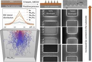
Until now there is no systematic study on the effect of the substrate type on the hydrogen silsesquioxane (HSQ) electron beam lithography (EBL) patterning process. We investigate arrays of line structures with varying width and spacing, starting at 10 nm, exposed at varying dose, and developed by salty NaOH and TMAH developers on group IV semiconductor substrates. We demonstrate that the HSQ EBL process on Ge is much more limited in achieving the smallest obtainable features, having optimal uniformity and fidelity, in comparison to Si. Monte-Carlo simulations of the e-beam/substrate interactions for “pure” Si and Ge substrates, and varying content Ge/Si epitaxial layers on Si, suggest that the limitations seen are directly linked to back-scattered electron (BSE) generation. As predicted by the simulations and shown experimentally, improved fidelity and resolution of the features can be achieved by minimizing the (BSE) generation coming from the Ge contribution in the substartes. Finally, from a metrology perspective, it is demonstrated that although line patterns may appear resolved in SEM images, the variation in the brightness across neighbouring lines is a key parameter in understanding the resist clearance between lines, that will affect the next etching step for pattern transfer onto the underlying substrate. These results are important for patterning high-density line structures and nano-device engineering as required for realising state-of-the art laterally stacked group IV multi-channel field effect transistors (FETs).
期刊介绍:
Microelectronic Engineering is the premier nanoprocessing, and nanotechnology journal focusing on fabrication of electronic, photonic, bioelectronic, electromechanic and fluidic devices and systems, and their applications in the broad areas of electronics, photonics, energy, life sciences, and environment. It covers also the expanding interdisciplinary field of "more than Moore" and "beyond Moore" integrated nanoelectronics / photonics and micro-/nano-/bio-systems. Through its unique mixture of peer-reviewed articles, reviews, accelerated publications, short and Technical notes, and the latest research news on key developments, Microelectronic Engineering provides comprehensive coverage of this exciting, interdisciplinary and dynamic new field for researchers in academia and professionals in industry.
 求助内容:
求助内容: 应助结果提醒方式:


