低温STM超导纳米结构的非原位制备

IF 4.6 2区 化学 Q2 CHEMISTRY, PHYSICAL
Adrian Greichgauer, Roozbeh Yazdanpanah, Alexey Taskin, Oliver Breunig, Yoichi Ando, Jens Brede
{"title":"低温STM超导纳米结构的非原位制备","authors":"Adrian Greichgauer, Roozbeh Yazdanpanah, Alexey Taskin, Oliver Breunig, Yoichi Ando, Jens Brede","doi":"10.1021/acs.jpclett.5c02383","DOIUrl":null,"url":null,"abstract":"Nanofabrication of topological insulator (TI) devices is essential for accessing edge and interface states, but conventional lithography and etching compromise the atomically clean surfaces required for scanning tunneling microscopy and spectroscopy (STM/STS). We demonstrate a fabrication strategy that combines ex situ lithographic patterning with in situ ultrahigh-vacuum cleaving and flipping, yielding atomically clean, nanopatterned TI-superconductor heterostructures suitable for STM/STS. In Design I, nanoribbons were defined by etching trenches into a TI film and capping with Nb. This enabled spectroscopy on large areas, although edge quality was limited by etch debris. In Design II, local thinning defined buried nanoribbons within a continuous TI film, producing pristine planar surfaces. STM/STS revealed well-developed superconducting gaps in the surrounding film, with suppressed gaps on the nanoribbons, consistent with vertical proximity coupling. This approach establishes a reproducible pathway for high-resolution STM/STS studies of proximitized nanostructures, providing a scalable platform for exploring topological superconductivity.","PeriodicalId":62,"journal":{"name":"The Journal of Physical Chemistry Letters","volume":"18 1","pages":""},"PeriodicalIF":4.6000,"publicationDate":"2025-10-21","publicationTypes":"Journal Article","fieldsOfStudy":null,"isOpenAccess":false,"openAccessPdf":"","citationCount":"0","resultStr":"{\"title\":\"Ex Situ Fabrication of Superconducting Nanostructures for Low-Temperature STM\",\"authors\":\"Adrian Greichgauer, Roozbeh Yazdanpanah, Alexey Taskin, Oliver Breunig, Yoichi Ando, Jens Brede\",\"doi\":\"10.1021/acs.jpclett.5c02383\",\"DOIUrl\":null,\"url\":null,\"abstract\":\"Nanofabrication of topological insulator (TI) devices is essential for accessing edge and interface states, but conventional lithography and etching compromise the atomically clean surfaces required for scanning tunneling microscopy and spectroscopy (STM/STS). We demonstrate a fabrication strategy that combines ex situ lithographic patterning with in situ ultrahigh-vacuum cleaving and flipping, yielding atomically clean, nanopatterned TI-superconductor heterostructures suitable for STM/STS. In Design I, nanoribbons were defined by etching trenches into a TI film and capping with Nb. This enabled spectroscopy on large areas, although edge quality was limited by etch debris. In Design II, local thinning defined buried nanoribbons within a continuous TI film, producing pristine planar surfaces. STM/STS revealed well-developed superconducting gaps in the surrounding film, with suppressed gaps on the nanoribbons, consistent with vertical proximity coupling. This approach establishes a reproducible pathway for high-resolution STM/STS studies of proximitized nanostructures, providing a scalable platform for exploring topological superconductivity.\",\"PeriodicalId\":62,\"journal\":{\"name\":\"The Journal of Physical Chemistry Letters\",\"volume\":\"18 1\",\"pages\":\"\"},\"PeriodicalIF\":4.6000,\"publicationDate\":\"2025-10-21\",\"publicationTypes\":\"Journal Article\",\"fieldsOfStudy\":null,\"isOpenAccess\":false,\"openAccessPdf\":\"\",\"citationCount\":\"0\",\"resultStr\":null,\"platform\":\"Semanticscholar\",\"paperid\":null,\"PeriodicalName\":\"The Journal of Physical Chemistry Letters\",\"FirstCategoryId\":\"1\",\"ListUrlMain\":\"https://doi.org/10.1021/acs.jpclett.5c02383\",\"RegionNum\":2,\"RegionCategory\":\"化学\",\"ArticlePicture\":[],\"TitleCN\":null,\"AbstractTextCN\":null,\"PMCID\":null,\"EPubDate\":\"\",\"PubModel\":\"\",\"JCR\":\"Q2\",\"JCRName\":\"CHEMISTRY, PHYSICAL\",\"Score\":null,\"Total\":0}","platform":"Semanticscholar","paperid":null,"PeriodicalName":"The Journal of Physical Chemistry Letters","FirstCategoryId":"1","ListUrlMain":"https://doi.org/10.1021/acs.jpclett.5c02383","RegionNum":2,"RegionCategory":"化学","ArticlePicture":[],"TitleCN":null,"AbstractTextCN":null,"PMCID":null,"EPubDate":"","PubModel":"","JCR":"Q2","JCRName":"CHEMISTRY, PHYSICAL","Score":null,"Total":0}
引用次数: 0

摘要

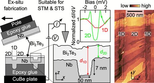
拓扑绝缘体(TI)器件的纳米制造对于获取边缘和界面状态至关重要,但传统的光刻和蚀刻损害了扫描隧道显微镜和光谱学(STM/STS)所需的原子清洁表面。我们展示了一种将非原位光刻图图化与原位超高真空切割和翻转相结合的制造策略,可以产生适合STM/STS的原子清洁,纳米图案ti -超导体异质结构。在设计I中,通过在TI薄膜上蚀刻沟槽并加盖Nb来定义纳米带。虽然边缘质量受到蚀刻碎片的限制,但这使光谱能够在大面积上进行。在设计II中,局部变薄定义了连续TI薄膜内埋藏的纳米带,产生原始的平面表面。STM/STS在周围薄膜中发现了发育良好的超导间隙,纳米带上的间隙被抑制,与垂直接近耦合一致。该方法为高分辨率STM/STS研究近似纳米结构建立了一个可重复的途径,为探索拓扑超导性提供了一个可扩展的平台。
本文章由计算机程序翻译,如有差异,请以英文原文为准。

Ex Situ Fabrication of Superconducting Nanostructures for Low-Temperature STM

Ex Situ Fabrication of Superconducting Nanostructures for Low-Temperature STM
Nanofabrication of topological insulator (TI) devices is essential for accessing edge and interface states, but conventional lithography and etching compromise the atomically clean surfaces required for scanning tunneling microscopy and spectroscopy (STM/STS). We demonstrate a fabrication strategy that combines ex situ lithographic patterning with in situ ultrahigh-vacuum cleaving and flipping, yielding atomically clean, nanopatterned TI-superconductor heterostructures suitable for STM/STS. In Design I, nanoribbons were defined by etching trenches into a TI film and capping with Nb. This enabled spectroscopy on large areas, although edge quality was limited by etch debris. In Design II, local thinning defined buried nanoribbons within a continuous TI film, producing pristine planar surfaces. STM/STS revealed well-developed superconducting gaps in the surrounding film, with suppressed gaps on the nanoribbons, consistent with vertical proximity coupling. This approach establishes a reproducible pathway for high-resolution STM/STS studies of proximitized nanostructures, providing a scalable platform for exploring topological superconductivity.
求助全文
通过发布文献求助,成功后即可免费获取论文全文。 去求助
来源期刊
The Journal of Physical Chemistry Letters
The Journal of Physical Chemistry Letters CHEMISTRY, PHYSICAL-NANOSCIENCE & NANOTECHNOLOGY
CiteScore
9.60
自引率
7.00%
发文量
1519
审稿时长
1.6 months
期刊介绍: The Journal of Physical Chemistry (JPC) Letters is devoted to reporting new and original experimental and theoretical basic research of interest to physical chemists, biophysical chemists, chemical physicists, physicists, material scientists, and engineers. An important criterion for acceptance is that the paper reports a significant scientific advance and/or physical insight such that rapid publication is essential. Two issues of JPC Letters are published each month.
×
引用
GB/T 7714-2015
复制
MLA
复制
APA
复制
导出至
BibTeX EndNote RefMan NoteFirst NoteExpress
×
提示
您的信息不完整,为了账户安全,请先补充。
现在去补充
×
提示
您因"违规操作"
具体请查看互助需知
我知道了
×
提示
确定
请完成安全验证×
copy
已复制链接
快去分享给好友吧!
我知道了
右上角分享
点击右上角分享
0
联系我们:info@booksci.cn Book学术提供免费学术资源搜索服务,方便国内外学者检索中英文文献。致力于提供最便捷和优质的服务体验。 Copyright © 2023 布克学术 All rights reserved.
京ICP备2023020795号-1
ghs 京公网安备 11010802042870号
Book学术文献互助
Book学术文献互助群
群 号:604180095
Book学术官方微信