利用深紫外光刻技术制备双波段红外元光学器件

IF 16 1区 材料科学 Q1 CHEMISTRY, MULTIDISCIPLINARY
ACS Nano Pub Date : 2025-10-19 DOI:10.1021/acsnano.5c11908
Kai Sun, Xingzhao Yan, Jordan Scott, Jun-Yu Ou, James N. Monks, Otto L. Muskens
{"title":"利用深紫外光刻技术制备双波段红外元光学器件","authors":"Kai Sun, Xingzhao Yan, Jordan Scott, Jun-Yu Ou, James N. Monks, Otto L. Muskens","doi":"10.1021/acsnano.5c11908","DOIUrl":null,"url":null,"abstract":"Metaoptics, the application of metasurfaces into optical systems, is seeing an accelerating development owing to advantages in size, weight, and cost and the ability to program optical functions beyond traditional refractive optics. The transition of metaoptics from the laboratory into applications is enabled by scalable production methods based on highly reproducible semiconductor process technology. Here, we introduce a method for the fabrication of double-sided metasurfaces through deep-UV lithography as a production-ready method for achieving high-quality metaoptics. We achieve patterning of a silicon wafer on both sides with mutual alignment of around 10 μm based on tool accuracy without requiring through-wafer alignment markers other than the wafer notch. An application highlighting the benefits of double-sided design is demonstrated in the form of a dual-band metalens with independent control over focal lengths in mid- and long-wavelength infrared bands. Using multireticle stitching, we demonstrate a 40 mm diameter, large-area metalens with excellent broadband imaging performance, showing partial canceling of chromatic dispersion when used in a hybrid configuration with a BaF<sub>2</sub> refractive lens. Our work establishes a production-ready approach to infrared metaoptics designs and double-sided metaoptics fabrication with direct potential for translation into scalable technology for real-world applications.","PeriodicalId":21,"journal":{"name":"ACS Nano","volume":"98 1","pages":""},"PeriodicalIF":16.0000,"publicationDate":"2025-10-19","publicationTypes":"Journal Article","fieldsOfStudy":null,"isOpenAccess":false,"openAccessPdf":"","citationCount":"0","resultStr":"{\"title\":\"Production-Ready Double-Sided Fabrication of Dual-Band Infrared Metaoptics Using Deep-Ultraviolet Lithography\",\"authors\":\"Kai Sun, Xingzhao Yan, Jordan Scott, Jun-Yu Ou, James N. Monks, Otto L. Muskens\",\"doi\":\"10.1021/acsnano.5c11908\",\"DOIUrl\":null,\"url\":null,\"abstract\":\"Metaoptics, the application of metasurfaces into optical systems, is seeing an accelerating development owing to advantages in size, weight, and cost and the ability to program optical functions beyond traditional refractive optics. The transition of metaoptics from the laboratory into applications is enabled by scalable production methods based on highly reproducible semiconductor process technology. Here, we introduce a method for the fabrication of double-sided metasurfaces through deep-UV lithography as a production-ready method for achieving high-quality metaoptics. We achieve patterning of a silicon wafer on both sides with mutual alignment of around 10 μm based on tool accuracy without requiring through-wafer alignment markers other than the wafer notch. An application highlighting the benefits of double-sided design is demonstrated in the form of a dual-band metalens with independent control over focal lengths in mid- and long-wavelength infrared bands. Using multireticle stitching, we demonstrate a 40 mm diameter, large-area metalens with excellent broadband imaging performance, showing partial canceling of chromatic dispersion when used in a hybrid configuration with a BaF<sub>2</sub> refractive lens. Our work establishes a production-ready approach to infrared metaoptics designs and double-sided metaoptics fabrication with direct potential for translation into scalable technology for real-world applications.\",\"PeriodicalId\":21,\"journal\":{\"name\":\"ACS Nano\",\"volume\":\"98 1\",\"pages\":\"\"},\"PeriodicalIF\":16.0000,\"publicationDate\":\"2025-10-19\",\"publicationTypes\":\"Journal Article\",\"fieldsOfStudy\":null,\"isOpenAccess\":false,\"openAccessPdf\":\"\",\"citationCount\":\"0\",\"resultStr\":null,\"platform\":\"Semanticscholar\",\"paperid\":null,\"PeriodicalName\":\"ACS Nano\",\"FirstCategoryId\":\"88\",\"ListUrlMain\":\"https://doi.org/10.1021/acsnano.5c11908\",\"RegionNum\":1,\"RegionCategory\":\"材料科学\",\"ArticlePicture\":[],\"TitleCN\":null,\"AbstractTextCN\":null,\"PMCID\":null,\"EPubDate\":\"\",\"PubModel\":\"\",\"JCR\":\"Q1\",\"JCRName\":\"CHEMISTRY, MULTIDISCIPLINARY\",\"Score\":null,\"Total\":0}","platform":"Semanticscholar","paperid":null,"PeriodicalName":"ACS Nano","FirstCategoryId":"88","ListUrlMain":"https://doi.org/10.1021/acsnano.5c11908","RegionNum":1,"RegionCategory":"材料科学","ArticlePicture":[],"TitleCN":null,"AbstractTextCN":null,"PMCID":null,"EPubDate":"","PubModel":"","JCR":"Q1","JCRName":"CHEMISTRY, MULTIDISCIPLINARY","Score":null,"Total":0}
引用次数: 0

摘要

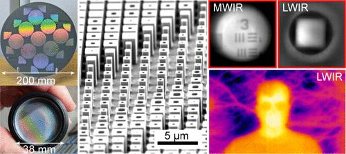
元光学(Metaoptics)是一种将超表面应用于光学系统的技术,由于其在尺寸、重量和成本方面的优势以及超越传统折射光学的编程光学功能的能力,正在加速发展。通过基于高度可复制的半导体工艺技术的可扩展生产方法,可使元光学从实验室过渡到应用。在这里,我们介绍了一种通过深紫外光刻制造双面超表面的方法,作为一种生产准备方法,以实现高质量的元光学。我们实现了硅晶圆两面的图像化,基于工具精度,相互对准约10 μm,而不需要晶圆缺口以外的晶圆对中标记。一个突出双面设计的优点的应用,以双波段超透镜的形式,在中长波红外波段具有独立的焦距控制。使用多线拼接,我们展示了40毫米直径,大面积超透镜具有优异的宽带成像性能,显示部分色散抵消与BaF2折射透镜的混合配置。我们的工作建立了一种生产就绪的红外元光学设计和双面元光学制造方法,具有直接转化为现实世界应用的可扩展技术的潜力。
本文章由计算机程序翻译,如有差异,请以英文原文为准。

Production-Ready Double-Sided Fabrication of Dual-Band Infrared Metaoptics Using Deep-Ultraviolet Lithography

Production-Ready Double-Sided Fabrication of Dual-Band Infrared Metaoptics Using Deep-Ultraviolet Lithography
Metaoptics, the application of metasurfaces into optical systems, is seeing an accelerating development owing to advantages in size, weight, and cost and the ability to program optical functions beyond traditional refractive optics. The transition of metaoptics from the laboratory into applications is enabled by scalable production methods based on highly reproducible semiconductor process technology. Here, we introduce a method for the fabrication of double-sided metasurfaces through deep-UV lithography as a production-ready method for achieving high-quality metaoptics. We achieve patterning of a silicon wafer on both sides with mutual alignment of around 10 μm based on tool accuracy without requiring through-wafer alignment markers other than the wafer notch. An application highlighting the benefits of double-sided design is demonstrated in the form of a dual-band metalens with independent control over focal lengths in mid- and long-wavelength infrared bands. Using multireticle stitching, we demonstrate a 40 mm diameter, large-area metalens with excellent broadband imaging performance, showing partial canceling of chromatic dispersion when used in a hybrid configuration with a BaF2 refractive lens. Our work establishes a production-ready approach to infrared metaoptics designs and double-sided metaoptics fabrication with direct potential for translation into scalable technology for real-world applications.
求助全文
通过发布文献求助,成功后即可免费获取论文全文。 去求助
来源期刊
ACS Nano
ACS Nano 工程技术-材料科学:综合
CiteScore
26.00
自引率
4.10%
发文量
1627
审稿时长
1.7 months
期刊介绍: ACS Nano, published monthly, serves as an international forum for comprehensive articles on nanoscience and nanotechnology research at the intersections of chemistry, biology, materials science, physics, and engineering. The journal fosters communication among scientists in these communities, facilitating collaboration, new research opportunities, and advancements through discoveries. ACS Nano covers synthesis, assembly, characterization, theory, and simulation of nanostructures, nanobiotechnology, nanofabrication, methods and tools for nanoscience and nanotechnology, and self- and directed-assembly. Alongside original research articles, it offers thorough reviews, perspectives on cutting-edge research, and discussions envisioning the future of nanoscience and nanotechnology.
×
引用
GB/T 7714-2015
复制
MLA
复制
APA
复制
导出至
BibTeX EndNote RefMan NoteFirst NoteExpress
×
提示
您的信息不完整,为了账户安全,请先补充。
现在去补充
×
提示
您因"违规操作"
具体请查看互助需知
我知道了
×
提示
确定
请完成安全验证×
copy
已复制链接
快去分享给好友吧!
我知道了
右上角分享
点击右上角分享
0
联系我们:info@booksci.cn Book学术提供免费学术资源搜索服务,方便国内外学者检索中英文文献。致力于提供最便捷和优质的服务体验。 Copyright © 2023 布克学术 All rights reserved.
京ICP备2023020795号-1
ghs 京公网安备 11010802042870号
Book学术文献互助
Book学术文献互助群
群 号:604180095
Book学术官方微信