倾斜结构的短通道二维场效应管

IF 8.2 2区 材料科学 Q1 MATERIALS SCIENCE, MULTIDISCIPLINARY
Junsung Byeon, Jinhyeok Pyo, Jungmoon Lim, Jaesik Eom, Byeongchan Kim, Min Jung, Hyungchang Jeong, Kyung-Ho Park, Sangyeon Pak, SeungNam Cha
{"title":"倾斜结构的短通道二维场效应管","authors":"Junsung Byeon, Jinhyeok Pyo, Jungmoon Lim, Jaesik Eom, Byeongchan Kim, Min Jung, Hyungchang Jeong, Kyung-Ho Park, Sangyeon Pak, SeungNam Cha","doi":"10.1021/acsami.5c18886","DOIUrl":null,"url":null,"abstract":"The miniaturization of electronic devices remains a primary focus in the semiconductor industry as it directly impacts both performance enhancement and cost reduction. However, achieving extreme scaling down often relies on high-resolution lithography techniques, which are limited by complexity and an intensive processing time. Two-dimensional transition metal dichalcogenides (2D TMDCs) have great potential for developing short-channel field effect transistors (FETs) due to their atomically thin nature and high Young’s modulus. Here, the nanometer-scale channel length in a 2D TMDC-based FET is realized by constructing the sloped architecture without lithography techniques. Utilizing h-BN tunneling layers ensures the mitigated short channel effect (SCE), resulting in a high on-off ratio and low subthreshold swing (SS). This sloped architecture short channel FET (SSFET) exhibits an on–off ratio over 10<sup>5</sup> with an SS of 160 mV/dec and an on-current level of 3.70 μA. This new approach can provide an innovative pathway to realize the nanometer-scale FET without complicating fabrication processes.","PeriodicalId":5,"journal":{"name":"ACS Applied Materials & Interfaces","volume":"12 1","pages":""},"PeriodicalIF":8.2000,"publicationDate":"2025-10-17","publicationTypes":"Journal Article","fieldsOfStudy":null,"isOpenAccess":false,"openAccessPdf":"","citationCount":"0","resultStr":"{\"title\":\"Short Channel 2D FET with Sloped Architecture\",\"authors\":\"Junsung Byeon, Jinhyeok Pyo, Jungmoon Lim, Jaesik Eom, Byeongchan Kim, Min Jung, Hyungchang Jeong, Kyung-Ho Park, Sangyeon Pak, SeungNam Cha\",\"doi\":\"10.1021/acsami.5c18886\",\"DOIUrl\":null,\"url\":null,\"abstract\":\"The miniaturization of electronic devices remains a primary focus in the semiconductor industry as it directly impacts both performance enhancement and cost reduction. However, achieving extreme scaling down often relies on high-resolution lithography techniques, which are limited by complexity and an intensive processing time. Two-dimensional transition metal dichalcogenides (2D TMDCs) have great potential for developing short-channel field effect transistors (FETs) due to their atomically thin nature and high Young’s modulus. Here, the nanometer-scale channel length in a 2D TMDC-based FET is realized by constructing the sloped architecture without lithography techniques. Utilizing h-BN tunneling layers ensures the mitigated short channel effect (SCE), resulting in a high on-off ratio and low subthreshold swing (SS). This sloped architecture short channel FET (SSFET) exhibits an on–off ratio over 10<sup>5</sup> with an SS of 160 mV/dec and an on-current level of 3.70 μA. This new approach can provide an innovative pathway to realize the nanometer-scale FET without complicating fabrication processes.\",\"PeriodicalId\":5,\"journal\":{\"name\":\"ACS Applied Materials & Interfaces\",\"volume\":\"12 1\",\"pages\":\"\"},\"PeriodicalIF\":8.2000,\"publicationDate\":\"2025-10-17\",\"publicationTypes\":\"Journal Article\",\"fieldsOfStudy\":null,\"isOpenAccess\":false,\"openAccessPdf\":\"\",\"citationCount\":\"0\",\"resultStr\":null,\"platform\":\"Semanticscholar\",\"paperid\":null,\"PeriodicalName\":\"ACS Applied Materials & Interfaces\",\"FirstCategoryId\":\"88\",\"ListUrlMain\":\"https://doi.org/10.1021/acsami.5c18886\",\"RegionNum\":2,\"RegionCategory\":\"材料科学\",\"ArticlePicture\":[],\"TitleCN\":null,\"AbstractTextCN\":null,\"PMCID\":null,\"EPubDate\":\"\",\"PubModel\":\"\",\"JCR\":\"Q1\",\"JCRName\":\"MATERIALS SCIENCE, MULTIDISCIPLINARY\",\"Score\":null,\"Total\":0}","platform":"Semanticscholar","paperid":null,"PeriodicalName":"ACS Applied Materials & Interfaces","FirstCategoryId":"88","ListUrlMain":"https://doi.org/10.1021/acsami.5c18886","RegionNum":2,"RegionCategory":"材料科学","ArticlePicture":[],"TitleCN":null,"AbstractTextCN":null,"PMCID":null,"EPubDate":"","PubModel":"","JCR":"Q1","JCRName":"MATERIALS SCIENCE, MULTIDISCIPLINARY","Score":null,"Total":0}
引用次数: 0

摘要

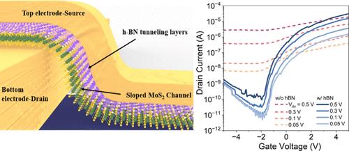
电子器件的小型化仍然是半导体工业的主要焦点,因为它直接影响到性能的提高和成本的降低。然而,实现极端缩小通常依赖于高分辨率光刻技术,这受到复杂性和密集处理时间的限制。二维过渡金属二硫族化合物(2D TMDCs)由于其原子薄的性质和高的杨氏模量,在短通道场效应晶体管(fet)中具有很大的发展潜力。在这里,在二维tmdc FET中,纳米尺度的通道长度是通过构建不使用光刻技术的倾斜结构来实现的。利用h-BN隧道层可确保减轻短信道效应(SCE),从而实现高开关比和低亚阈值摆幅(SS)。这种倾斜结构的短通道FET (SSFET)的通断比超过105,SS为160 mV/dec,导通电流水平为3.70 μA。这种新方法为实现纳米级场效应管提供了一条创新的途径,而无需复杂的制造工艺。
本文章由计算机程序翻译,如有差异,请以英文原文为准。

Short Channel 2D FET with Sloped Architecture

Short Channel 2D FET with Sloped Architecture
The miniaturization of electronic devices remains a primary focus in the semiconductor industry as it directly impacts both performance enhancement and cost reduction. However, achieving extreme scaling down often relies on high-resolution lithography techniques, which are limited by complexity and an intensive processing time. Two-dimensional transition metal dichalcogenides (2D TMDCs) have great potential for developing short-channel field effect transistors (FETs) due to their atomically thin nature and high Young’s modulus. Here, the nanometer-scale channel length in a 2D TMDC-based FET is realized by constructing the sloped architecture without lithography techniques. Utilizing h-BN tunneling layers ensures the mitigated short channel effect (SCE), resulting in a high on-off ratio and low subthreshold swing (SS). This sloped architecture short channel FET (SSFET) exhibits an on–off ratio over 105 with an SS of 160 mV/dec and an on-current level of 3.70 μA. This new approach can provide an innovative pathway to realize the nanometer-scale FET without complicating fabrication processes.
求助全文
通过发布文献求助,成功后即可免费获取论文全文。 去求助
来源期刊
ACS Applied Materials & Interfaces
ACS Applied Materials & Interfaces 工程技术-材料科学:综合
CiteScore
16.00
自引率
6.30%
发文量
4978
审稿时长
1.8 months
期刊介绍: ACS Applied Materials & Interfaces is a leading interdisciplinary journal that brings together chemists, engineers, physicists, and biologists to explore the development and utilization of newly-discovered materials and interfacial processes for specific applications. Our journal has experienced remarkable growth since its establishment in 2009, both in terms of the number of articles published and the impact of the research showcased. We are proud to foster a truly global community, with the majority of published articles originating from outside the United States, reflecting the rapid growth of applied research worldwide.
×
引用
GB/T 7714-2015
复制
MLA
复制
APA
复制
导出至
BibTeX EndNote RefMan NoteFirst NoteExpress
×
提示
您的信息不完整,为了账户安全,请先补充。
现在去补充
×
提示
您因"违规操作"
具体请查看互助需知
我知道了
×
提示
确定
请完成安全验证×
copy
已复制链接
快去分享给好友吧!
我知道了
右上角分享
点击右上角分享
0
联系我们:info@booksci.cn Book学术提供免费学术资源搜索服务,方便国内外学者检索中英文文献。致力于提供最便捷和优质的服务体验。 Copyright © 2023 布克学术 All rights reserved.
京ICP备2023020795号-1
ghs 京公网安备 11010802042870号
Book学术文献互助
Book学术文献互助群
群 号:604180095
Book学术官方微信