Sungmin Yoon, Seokhoon Choi, Min-Hyun Lee, Sunho Kim, Seonghoon Jang, Hyunseong Park, Dooho Lee, Seung-Yeul Yang, Jeong Young Park
{"title":"利用开尔文探针力显微镜研究氧化氮氧化物堆中埋藏电荷阱的纳米级动力学。","authors":"Sungmin Yoon, Seokhoon Choi, Min-Hyun Lee, Sunho Kim, Seonghoon Jang, Hyunseong Park, Dooho Lee, Seung-Yeul Yang, Jeong Young Park","doi":"10.1021/acs.nanolett.5c03652","DOIUrl":null,"url":null,"abstract":"<p><p>Understanding charge trapping and diffusion behavior is crucial for optimizing nonvolatile memory (NVM) devices, which commercially involve a silicon oxide-silicon nitride-silicon oxide (ONO) stack structure. However, studies on charge traps in ONO stack structures using Kelvin probe force microscopy (KPFM) have been limited. Here, we examine trapped charge dynamics in ONO devices using KPFM, especially trapped electrons and holes in the buried silicon nitride layer and on the exposed silicon oxide. Furthermore, we observe diffusion of trapped holes on the exposed oxide and electron diffusion within the buried nitride during the program process. As a result, the diffusion coefficients are quantified as 5.20 × 10<sup>-13</sup> cm<sup>2</sup>/s for holes trapped in the exposed oxide layer and 1.22 × 10<sup>-14</sup> cm<sup>2</sup>/s for electrons trapped in the subsurface nitride layer. Hence, we identify distinct charge dissipation in buried and surface layers, demonstrating the capability of KPFM to characterize charge-trap materials and improve NVM devices.</p>","PeriodicalId":53,"journal":{"name":"Nano Letters","volume":" ","pages":""},"PeriodicalIF":9.1000,"publicationDate":"2025-10-09","publicationTypes":"Journal Article","fieldsOfStudy":null,"isOpenAccess":false,"openAccessPdf":"","citationCount":"0","resultStr":"{\"title\":\"Nanoscale Dynamics of Buried Charge Trap in Oxide-Nitride-Oxide Stacks Investigated Using Kelvin Probe Force Microscopy.\",\"authors\":\"Sungmin Yoon, Seokhoon Choi, Min-Hyun Lee, Sunho Kim, Seonghoon Jang, Hyunseong Park, Dooho Lee, Seung-Yeul Yang, Jeong Young Park\",\"doi\":\"10.1021/acs.nanolett.5c03652\",\"DOIUrl\":null,\"url\":null,\"abstract\":\"<p><p>Understanding charge trapping and diffusion behavior is crucial for optimizing nonvolatile memory (NVM) devices, which commercially involve a silicon oxide-silicon nitride-silicon oxide (ONO) stack structure. However, studies on charge traps in ONO stack structures using Kelvin probe force microscopy (KPFM) have been limited. Here, we examine trapped charge dynamics in ONO devices using KPFM, especially trapped electrons and holes in the buried silicon nitride layer and on the exposed silicon oxide. Furthermore, we observe diffusion of trapped holes on the exposed oxide and electron diffusion within the buried nitride during the program process. As a result, the diffusion coefficients are quantified as 5.20 × 10<sup>-13</sup> cm<sup>2</sup>/s for holes trapped in the exposed oxide layer and 1.22 × 10<sup>-14</sup> cm<sup>2</sup>/s for electrons trapped in the subsurface nitride layer. Hence, we identify distinct charge dissipation in buried and surface layers, demonstrating the capability of KPFM to characterize charge-trap materials and improve NVM devices.</p>\",\"PeriodicalId\":53,\"journal\":{\"name\":\"Nano Letters\",\"volume\":\" \",\"pages\":\"\"},\"PeriodicalIF\":9.1000,\"publicationDate\":\"2025-10-09\",\"publicationTypes\":\"Journal Article\",\"fieldsOfStudy\":null,\"isOpenAccess\":false,\"openAccessPdf\":\"\",\"citationCount\":\"0\",\"resultStr\":null,\"platform\":\"Semanticscholar\",\"paperid\":null,\"PeriodicalName\":\"Nano Letters\",\"FirstCategoryId\":\"88\",\"ListUrlMain\":\"https://doi.org/10.1021/acs.nanolett.5c03652\",\"RegionNum\":1,\"RegionCategory\":\"材料科学\",\"ArticlePicture\":[],\"TitleCN\":null,\"AbstractTextCN\":null,\"PMCID\":null,\"EPubDate\":\"\",\"PubModel\":\"\",\"JCR\":\"Q1\",\"JCRName\":\"CHEMISTRY, MULTIDISCIPLINARY\",\"Score\":null,\"Total\":0}","platform":"Semanticscholar","paperid":null,"PeriodicalName":"Nano Letters","FirstCategoryId":"88","ListUrlMain":"https://doi.org/10.1021/acs.nanolett.5c03652","RegionNum":1,"RegionCategory":"材料科学","ArticlePicture":[],"TitleCN":null,"AbstractTextCN":null,"PMCID":null,"EPubDate":"","PubModel":"","JCR":"Q1","JCRName":"CHEMISTRY, MULTIDISCIPLINARY","Score":null,"Total":0}
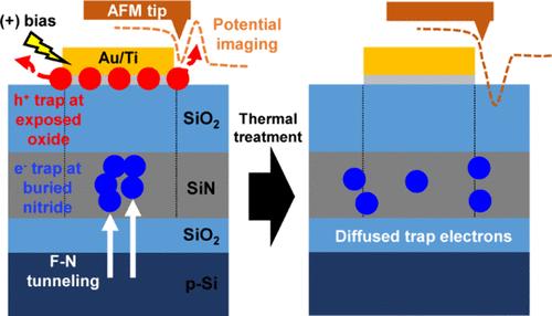
Nanoscale Dynamics of Buried Charge Trap in Oxide-Nitride-Oxide Stacks Investigated Using Kelvin Probe Force Microscopy.
Understanding charge trapping and diffusion behavior is crucial for optimizing nonvolatile memory (NVM) devices, which commercially involve a silicon oxide-silicon nitride-silicon oxide (ONO) stack structure. However, studies on charge traps in ONO stack structures using Kelvin probe force microscopy (KPFM) have been limited. Here, we examine trapped charge dynamics in ONO devices using KPFM, especially trapped electrons and holes in the buried silicon nitride layer and on the exposed silicon oxide. Furthermore, we observe diffusion of trapped holes on the exposed oxide and electron diffusion within the buried nitride during the program process. As a result, the diffusion coefficients are quantified as 5.20 × 10⁻¹³ cm2/s for holes trapped in the exposed oxide layer and 1.22 × 10⁻¹⁴ cm2/s for electrons trapped in the subsurface nitride layer. Hence, we identify distinct charge dissipation in buried and surface layers, demonstrating the capability of KPFM to characterize charge-trap materials and improve NVM devices.
期刊介绍:
Nano Letters serves as a dynamic platform for promptly disseminating original results in fundamental, applied, and emerging research across all facets of nanoscience and nanotechnology. A pivotal criterion for inclusion within Nano Letters is the convergence of at least two different areas or disciplines, ensuring a rich interdisciplinary scope. The journal is dedicated to fostering exploration in diverse areas, including:
- Experimental and theoretical findings on physical, chemical, and biological phenomena at the nanoscale
- Synthesis, characterization, and processing of organic, inorganic, polymer, and hybrid nanomaterials through physical, chemical, and biological methodologies
- Modeling and simulation of synthetic, assembly, and interaction processes
- Realization of integrated nanostructures and nano-engineered devices exhibiting advanced performance
- Applications of nanoscale materials in living and environmental systems
Nano Letters is committed to advancing and showcasing groundbreaking research that intersects various domains, fostering innovation and collaboration in the ever-evolving field of nanoscience and nanotechnology.

 求助内容:
求助内容: 应助结果提醒方式:


