{"title":"通过冷却增强单晶MAPbI3纳米线的弱光检测","authors":"Yue Han, , , Rui Gao, , , Wenbo Zeng, , , Yuying Xi, , , Chen Tang, , , Ting Ji, , , Yanxia Cui*, , and , Guohui Li*, ","doi":"10.1021/acsanm.5c02404","DOIUrl":null,"url":null,"abstract":"<p >Photodetectors (PDs) capable of detecting weak light are critical for applications like astronomical observation, quantum computing, cryogenic biomedical imaging, material analysis and precision measurements. Perovskite materials, due to their high carrier mobility, long diffusion lengths, and solution processability, offer substantial advantages in PD performance. In this study, we fabricated high-quality single-crystalline nanowires (NWs) of methylammonium lead iodide (MAPbI<sub>3</sub>) and developed a high-performance metal–semiconductor-metal PD operating at 85 K. The device demonstrated an extremely low dark current of 3.7 × 10<sup>–13</sup> A (1 V) at 85 K, 4 orders of magnitude lower than at room temperature (RT). Its detectivity exceeded RT performance by a factor of 706, reaching 7.7 × 10<sup>13</sup> Jones, and achieved a phototo-dark current ratio exceeding 10<sup>8</sup> under 532 nm light illumination at 204 mW/cm<sup>2</sup>. As the optical power density decreased to 12 nW/cm<sup>2</sup>, detectivity further increased to 2.7 × 10<sup>15</sup> Jones. These improvements are linked to the phase transition from tetragonal to orthorhombic crystal structure, which results in a widened bandgap. At 85 K, thermally excited carriers and ion migration are significantly suppressed, and defect self-annihilation is promoted, leading to a much-reduced dark current. Additionally, the reduced defects lower nonradiative recombination and the ordered molecular arrangement could enhance the generation and transport of photogenerated charge carriers under illumination with a power density above 40 μW/cm<sup>2</sup> (532 nm) at 85 K. This work sets a benchmark for MAPbI<sub>3</sub> PD performance, demonstrating the potential of perovskite-based devices for weak light detection.</p>","PeriodicalId":6,"journal":{"name":"ACS Applied Nano Materials","volume":"8 40","pages":"19135–19144"},"PeriodicalIF":5.5000,"publicationDate":"2025-09-25","publicationTypes":"Journal Article","fieldsOfStudy":null,"isOpenAccess":false,"openAccessPdf":"","citationCount":"0","resultStr":"{\"title\":\"Enhancing Weak Light Detection in Single-Crystalline MAPbI3 Nanowires via Cooling\",\"authors\":\"Yue Han, , , Rui Gao, , , Wenbo Zeng, , , Yuying Xi, , , Chen Tang, , , Ting Ji, , , Yanxia Cui*, , and , Guohui Li*, \",\"doi\":\"10.1021/acsanm.5c02404\",\"DOIUrl\":null,\"url\":null,\"abstract\":\"<p >Photodetectors (PDs) capable of detecting weak light are critical for applications like astronomical observation, quantum computing, cryogenic biomedical imaging, material analysis and precision measurements. Perovskite materials, due to their high carrier mobility, long diffusion lengths, and solution processability, offer substantial advantages in PD performance. In this study, we fabricated high-quality single-crystalline nanowires (NWs) of methylammonium lead iodide (MAPbI<sub>3</sub>) and developed a high-performance metal–semiconductor-metal PD operating at 85 K. The device demonstrated an extremely low dark current of 3.7 × 10<sup>–13</sup> A (1 V) at 85 K, 4 orders of magnitude lower than at room temperature (RT). Its detectivity exceeded RT performance by a factor of 706, reaching 7.7 × 10<sup>13</sup> Jones, and achieved a phototo-dark current ratio exceeding 10<sup>8</sup> under 532 nm light illumination at 204 mW/cm<sup>2</sup>. As the optical power density decreased to 12 nW/cm<sup>2</sup>, detectivity further increased to 2.7 × 10<sup>15</sup> Jones. These improvements are linked to the phase transition from tetragonal to orthorhombic crystal structure, which results in a widened bandgap. At 85 K, thermally excited carriers and ion migration are significantly suppressed, and defect self-annihilation is promoted, leading to a much-reduced dark current. Additionally, the reduced defects lower nonradiative recombination and the ordered molecular arrangement could enhance the generation and transport of photogenerated charge carriers under illumination with a power density above 40 μW/cm<sup>2</sup> (532 nm) at 85 K. This work sets a benchmark for MAPbI<sub>3</sub> PD performance, demonstrating the potential of perovskite-based devices for weak light detection.</p>\",\"PeriodicalId\":6,\"journal\":{\"name\":\"ACS Applied Nano Materials\",\"volume\":\"8 40\",\"pages\":\"19135–19144\"},\"PeriodicalIF\":5.5000,\"publicationDate\":\"2025-09-25\",\"publicationTypes\":\"Journal Article\",\"fieldsOfStudy\":null,\"isOpenAccess\":false,\"openAccessPdf\":\"\",\"citationCount\":\"0\",\"resultStr\":null,\"platform\":\"Semanticscholar\",\"paperid\":null,\"PeriodicalName\":\"ACS Applied Nano Materials\",\"FirstCategoryId\":\"88\",\"ListUrlMain\":\"https://pubs.acs.org/doi/10.1021/acsanm.5c02404\",\"RegionNum\":2,\"RegionCategory\":\"材料科学\",\"ArticlePicture\":[],\"TitleCN\":null,\"AbstractTextCN\":null,\"PMCID\":null,\"EPubDate\":\"\",\"PubModel\":\"\",\"JCR\":\"Q2\",\"JCRName\":\"MATERIALS SCIENCE, MULTIDISCIPLINARY\",\"Score\":null,\"Total\":0}","platform":"Semanticscholar","paperid":null,"PeriodicalName":"ACS Applied Nano Materials","FirstCategoryId":"88","ListUrlMain":"https://pubs.acs.org/doi/10.1021/acsanm.5c02404","RegionNum":2,"RegionCategory":"材料科学","ArticlePicture":[],"TitleCN":null,"AbstractTextCN":null,"PMCID":null,"EPubDate":"","PubModel":"","JCR":"Q2","JCRName":"MATERIALS SCIENCE, MULTIDISCIPLINARY","Score":null,"Total":0}
Enhancing Weak Light Detection in Single-Crystalline MAPbI3 Nanowires via Cooling
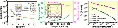
Photodetectors (PDs) capable of detecting weak light are critical for applications like astronomical observation, quantum computing, cryogenic biomedical imaging, material analysis and precision measurements. Perovskite materials, due to their high carrier mobility, long diffusion lengths, and solution processability, offer substantial advantages in PD performance. In this study, we fabricated high-quality single-crystalline nanowires (NWs) of methylammonium lead iodide (MAPbI3) and developed a high-performance metal–semiconductor-metal PD operating at 85 K. The device demonstrated an extremely low dark current of 3.7 × 10⁻¹³ A (1 V) at 85 K, 4 orders of magnitude lower than at room temperature (RT). Its detectivity exceeded RT performance by a factor of 706, reaching 7.7 × 10¹³ Jones, and achieved a phototo-dark current ratio exceeding 108 under 532 nm light illumination at 204 mW/cm2. As the optical power density decreased to 12 nW/cm2, detectivity further increased to 2.7 × 10¹⁵ Jones. These improvements are linked to the phase transition from tetragonal to orthorhombic crystal structure, which results in a widened bandgap. At 85 K, thermally excited carriers and ion migration are significantly suppressed, and defect self-annihilation is promoted, leading to a much-reduced dark current. Additionally, the reduced defects lower nonradiative recombination and the ordered molecular arrangement could enhance the generation and transport of photogenerated charge carriers under illumination with a power density above 40 μW/cm2 (532 nm) at 85 K. This work sets a benchmark for MAPbI3 PD performance, demonstrating the potential of perovskite-based devices for weak light detection.
期刊介绍:
ACS Applied Nano Materials is an interdisciplinary journal publishing original research covering all aspects of engineering, chemistry, physics and biology relevant to applications of nanomaterials. The journal is devoted to reports of new and original experimental and theoretical research of an applied nature that integrate knowledge in the areas of materials, engineering, physics, bioscience, and chemistry into important applications of nanomaterials.

 求助内容:
求助内容: 应助结果提醒方式:


