空气处理Sb2S3太阳能电池的界面工程方法,可实现7.5% AM 1.5G器件效率和18%室内里程碑性能

IF 9.5 2区 材料科学 Q1 CHEMISTRY, PHYSICAL
Hadeer Hussien, Malle Krunks, Nicolae Spalatu, Atanas Katerski, Zacharie Jehl Li-Kao, Sergio Giraldo, Daniel Abou-Ras, Arivazhagan Valluvar Oli, Susanne Siebentritt, Jonathan D. Major, Aeshah A. Almushawwah, Thomas P. Shalvey, Raitis Grzibovskis, Aivars Vembris, Ilona Oja Acik
{"title":"空气处理Sb2S3太阳能电池的界面工程方法,可实现7.5% AM 1.5G器件效率和18%室内里程碑性能","authors":"Hadeer Hussien, Malle Krunks, Nicolae Spalatu, Atanas Katerski, Zacharie Jehl Li-Kao, Sergio Giraldo, Daniel Abou-Ras, Arivazhagan Valluvar Oli, Susanne Siebentritt, Jonathan D. Major, Aeshah A. Almushawwah, Thomas P. Shalvey, Raitis Grzibovskis, Aivars Vembris, Ilona Oja Acik","doi":"10.1039/d5ta05790f","DOIUrl":null,"url":null,"abstract":"Among the wide range of emerging absorber materials under development, Sb<small><sub>2</sub></small>S<small><sub>3</sub></small>, with its optimal bandgap of 1.7 eV and distinctive anisotropic properties, stands out as a material offering an excellent trade-off between intrinsic stability, cost-effective deposition, and high performance under both, AM 1.5G and indoor illumination. While current strategies focus on absorber optimization, interface engineering remains largely unexplored. In this work, we introduce, for the first time, a ZnO interfacial layer deposited <em>via</em> ultrasonic spray pyrolysis (USP) in air at the TiO<small><sub>2</sub></small>/Sb<small><sub>2</sub></small>S<small><sub>3</sub></small> interface. This innovation extends to a fully cadmium-free device architecture, in which all key layers—TiO<small><sub>2</sub></small> electron transport layer, ZnO interlayer, and Sb<small><sub>2</sub></small>S<small><sub>3</sub></small> absorber—are processed entirely <em>via</em> USP under ambient conditions. A record efficiency of 7.5% under AM 1.5G illumination and an 18% indoor milestone performance is demonstrated for a TiO<small><sub>2</sub></small>-based Sb<small><sub>2</sub></small>S<small><sub>3</sub></small> solar cell platform, featuring a 150 nm thick absorber—the thinnest Sb<small><sub>2</sub></small>S<small><sub>3</sub></small> absorber delivering such performance to date. Comprehensive characterization reveals the critical role of the ZnO interfacial layer, highlighting its impact on absorber grain size, interface and bulk defects, and device functionality. We propose refinements to indoor measurement protocols, accounting for variations in source temperature and incident power, paving the way for reliable indoor PV performance evaluation.","PeriodicalId":82,"journal":{"name":"Journal of Materials Chemistry A","volume":"2 1","pages":""},"PeriodicalIF":9.5000,"publicationDate":"2025-10-09","publicationTypes":"Journal Article","fieldsOfStudy":null,"isOpenAccess":false,"openAccessPdf":"","citationCount":"0","resultStr":"{\"title\":\"Interface engineering approach of in-air-processed Sb2S3 solar cells enabling 7.5% AM 1.5G device efficiency and an 18% indoor milestone performance\",\"authors\":\"Hadeer Hussien, Malle Krunks, Nicolae Spalatu, Atanas Katerski, Zacharie Jehl Li-Kao, Sergio Giraldo, Daniel Abou-Ras, Arivazhagan Valluvar Oli, Susanne Siebentritt, Jonathan D. Major, Aeshah A. Almushawwah, Thomas P. Shalvey, Raitis Grzibovskis, Aivars Vembris, Ilona Oja Acik\",\"doi\":\"10.1039/d5ta05790f\",\"DOIUrl\":null,\"url\":null,\"abstract\":\"Among the wide range of emerging absorber materials under development, Sb<small><sub>2</sub></small>S<small><sub>3</sub></small>, with its optimal bandgap of 1.7 eV and distinctive anisotropic properties, stands out as a material offering an excellent trade-off between intrinsic stability, cost-effective deposition, and high performance under both, AM 1.5G and indoor illumination. While current strategies focus on absorber optimization, interface engineering remains largely unexplored. In this work, we introduce, for the first time, a ZnO interfacial layer deposited <em>via</em> ultrasonic spray pyrolysis (USP) in air at the TiO<small><sub>2</sub></small>/Sb<small><sub>2</sub></small>S<small><sub>3</sub></small> interface. This innovation extends to a fully cadmium-free device architecture, in which all key layers—TiO<small><sub>2</sub></small> electron transport layer, ZnO interlayer, and Sb<small><sub>2</sub></small>S<small><sub>3</sub></small> absorber—are processed entirely <em>via</em> USP under ambient conditions. A record efficiency of 7.5% under AM 1.5G illumination and an 18% indoor milestone performance is demonstrated for a TiO<small><sub>2</sub></small>-based Sb<small><sub>2</sub></small>S<small><sub>3</sub></small> solar cell platform, featuring a 150 nm thick absorber—the thinnest Sb<small><sub>2</sub></small>S<small><sub>3</sub></small> absorber delivering such performance to date. Comprehensive characterization reveals the critical role of the ZnO interfacial layer, highlighting its impact on absorber grain size, interface and bulk defects, and device functionality. We propose refinements to indoor measurement protocols, accounting for variations in source temperature and incident power, paving the way for reliable indoor PV performance evaluation.\",\"PeriodicalId\":82,\"journal\":{\"name\":\"Journal of Materials Chemistry A\",\"volume\":\"2 1\",\"pages\":\"\"},\"PeriodicalIF\":9.5000,\"publicationDate\":\"2025-10-09\",\"publicationTypes\":\"Journal Article\",\"fieldsOfStudy\":null,\"isOpenAccess\":false,\"openAccessPdf\":\"\",\"citationCount\":\"0\",\"resultStr\":null,\"platform\":\"Semanticscholar\",\"paperid\":null,\"PeriodicalName\":\"Journal of Materials Chemistry A\",\"FirstCategoryId\":\"88\",\"ListUrlMain\":\"https://doi.org/10.1039/d5ta05790f\",\"RegionNum\":2,\"RegionCategory\":\"材料科学\",\"ArticlePicture\":[],\"TitleCN\":null,\"AbstractTextCN\":null,\"PMCID\":null,\"EPubDate\":\"\",\"PubModel\":\"\",\"JCR\":\"Q1\",\"JCRName\":\"CHEMISTRY, PHYSICAL\",\"Score\":null,\"Total\":0}","platform":"Semanticscholar","paperid":null,"PeriodicalName":"Journal of Materials Chemistry A","FirstCategoryId":"88","ListUrlMain":"https://doi.org/10.1039/d5ta05790f","RegionNum":2,"RegionCategory":"材料科学","ArticlePicture":[],"TitleCN":null,"AbstractTextCN":null,"PMCID":null,"EPubDate":"","PubModel":"","JCR":"Q1","JCRName":"CHEMISTRY, PHYSICAL","Score":null,"Total":0}
引用次数: 0

摘要

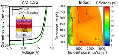
在众多正在开发的新兴吸收材料中,Sb2S3具有1.7 eV的最佳带隙和独特的各向异性特性,在AM 1.5G和室内照明下,作为一种在内在稳定性,成本效益沉积和高性能之间提供出色平衡的材料脱颖而出。虽然目前的策略主要集中在吸收剂优化上,但界面工程在很大程度上仍未得到探索。在这项工作中,我们首次在空气中通过超声波喷雾热解(USP)在TiO2/Sb2S3界面上沉积了ZnO界面层。这一创新扩展到完全无镉的器件架构,其中所有关键层- tio2电子传输层,ZnO中间层和Sb2S3吸收层-在环境条件下完全通过USP处理。基于tio2的Sb2S3太阳能电池平台在AM 1.5G照明下的效率达到创纪录的7.5%,室内里程碑性能达到18%,该平台具有150nm厚的吸收器,是迄今为止最薄的Sb2S3吸收器。综合表征揭示了ZnO界面层的关键作用,突出了它对吸收剂晶粒尺寸、界面和体积缺陷以及器件功能的影响。我们建议对室内测量方案进行改进,考虑源温度和入射功率的变化,为可靠的室内光伏性能评估铺平道路。
本文章由计算机程序翻译,如有差异,请以英文原文为准。

Interface engineering approach of in-air-processed Sb2S3 solar cells enabling 7.5% AM 1.5G device efficiency and an 18% indoor milestone performance

Interface engineering approach of in-air-processed Sb2S3 solar cells enabling 7.5% AM 1.5G device efficiency and an 18% indoor milestone performance
Among the wide range of emerging absorber materials under development, Sb2S3, with its optimal bandgap of 1.7 eV and distinctive anisotropic properties, stands out as a material offering an excellent trade-off between intrinsic stability, cost-effective deposition, and high performance under both, AM 1.5G and indoor illumination. While current strategies focus on absorber optimization, interface engineering remains largely unexplored. In this work, we introduce, for the first time, a ZnO interfacial layer deposited via ultrasonic spray pyrolysis (USP) in air at the TiO2/Sb2S3 interface. This innovation extends to a fully cadmium-free device architecture, in which all key layers—TiO2 electron transport layer, ZnO interlayer, and Sb2S3 absorber—are processed entirely via USP under ambient conditions. A record efficiency of 7.5% under AM 1.5G illumination and an 18% indoor milestone performance is demonstrated for a TiO2-based Sb2S3 solar cell platform, featuring a 150 nm thick absorber—the thinnest Sb2S3 absorber delivering such performance to date. Comprehensive characterization reveals the critical role of the ZnO interfacial layer, highlighting its impact on absorber grain size, interface and bulk defects, and device functionality. We propose refinements to indoor measurement protocols, accounting for variations in source temperature and incident power, paving the way for reliable indoor PV performance evaluation.
求助全文
通过发布文献求助,成功后即可免费获取论文全文。 去求助
来源期刊
Journal of Materials Chemistry A
Journal of Materials Chemistry A CHEMISTRY, PHYSICAL-ENERGY & FUELS
CiteScore
19.50
自引率
5.00%
发文量
1892
审稿时长
1.5 months
期刊介绍: The Journal of Materials Chemistry A, B & C covers a wide range of high-quality studies in the field of materials chemistry, with each section focusing on specific applications of the materials studied. Journal of Materials Chemistry A emphasizes applications in energy and sustainability, including topics such as artificial photosynthesis, batteries, and fuel cells. Journal of Materials Chemistry B focuses on applications in biology and medicine, while Journal of Materials Chemistry C covers applications in optical, magnetic, and electronic devices. Example topic areas within the scope of Journal of Materials Chemistry A include catalysis, green/sustainable materials, sensors, and water treatment, among others.
×
引用
GB/T 7714-2015
复制
MLA
复制
APA
复制
导出至
BibTeX EndNote RefMan NoteFirst NoteExpress
×
提示
您的信息不完整,为了账户安全,请先补充。
现在去补充
×
提示
您因"违规操作"
具体请查看互助需知
我知道了
×
提示
确定
请完成安全验证×
copy
已复制链接
快去分享给好友吧!
我知道了
右上角分享
点击右上角分享
0
联系我们:info@booksci.cn Book学术提供免费学术资源搜索服务,方便国内外学者检索中英文文献。致力于提供最便捷和优质的服务体验。 Copyright © 2023 布克学术 All rights reserved.
京ICP备2023020795号-1
ghs 京公网安备 11010802042870号
Book学术文献互助
Book学术文献互助群
群 号:604180095
Book学术官方微信