一种表征二维MoS2层的晶圆尺度方法

IF 6.9 2区 材料科学 Q2 CHEMISTRY, PHYSICAL
T. Meyer, S. Cadot, B. Dey, T. Vollaire, P. Brunet, P. Quéméré, N. Gauthier, V.-H. Le, D. Mariolle, H. Okuno, B. Smiri, T. Gouth, M. Pichois, E. Nolot, L. Le Van-Jodin
{"title":"一种表征二维MoS2层的晶圆尺度方法","authors":"T. Meyer, S. Cadot, B. Dey, T. Vollaire, P. Brunet, P. Quéméré, N. Gauthier, V.-H. Le, D. Mariolle, H. Okuno, B. Smiri, T. Gouth, M. Pichois, E. Nolot, L. Le Van-Jodin","doi":"10.1016/j.apsusc.2025.164785","DOIUrl":null,"url":null,"abstract":"Wafer-scale deposition of 2D TMDs (Transition Metal Dichalcogenides) is a key point for their integration in future devices. While significant efforts have been dedicated to improving the quality and uniformity of 2D materials, their implementation requires a robust characterization protocol to assess the surface coverage, layer number, stoichiometry, homogeneity, crystallinity and morphology. In this work, we developed a characterization protocol that combined local analyses and large-scale methods. This protocol was applied to MoS<sub>2</sub> films grown on SiO<sub>2</sub> substrate by Atomic Layer Deposition (ALD) using two different precursors, enabling the determination of the number of ALD cycles required to achieve a strict monolayer with full wafer-scale coverage. Atomic Force Microscopy (AFM), X-ray Photoelectron Spectroscopy (XPS), and Scanning Transmission Electron Microscopy (STEM) provided insights into composition, surface coverage and equivalent thickness from sub-monolayer to above-monolayer thickness range at low scale. The combination of Wavelength-Dispersive X-ray Fluorescence (WDXRF), Scanning Electron Microscopy (SEM), Raman spectroscopy and Photoluminescence, enables a rapid and accurate evaluation of the uniformity at wafer scale, the equivalent thickness and composition of TMD films across the wafer.","PeriodicalId":247,"journal":{"name":"Applied Surface Science","volume":"7 1","pages":""},"PeriodicalIF":6.9000,"publicationDate":"2025-10-08","publicationTypes":"Journal Article","fieldsOfStudy":null,"isOpenAccess":false,"openAccessPdf":"","citationCount":"0","resultStr":"{\"title\":\"A wafer-scale method for the characterization of 2D MoS2 layers\",\"authors\":\"T. Meyer, S. Cadot, B. Dey, T. Vollaire, P. Brunet, P. Quéméré, N. Gauthier, V.-H. Le, D. Mariolle, H. Okuno, B. Smiri, T. Gouth, M. Pichois, E. Nolot, L. Le Van-Jodin\",\"doi\":\"10.1016/j.apsusc.2025.164785\",\"DOIUrl\":null,\"url\":null,\"abstract\":\"Wafer-scale deposition of 2D TMDs (Transition Metal Dichalcogenides) is a key point for their integration in future devices. While significant efforts have been dedicated to improving the quality and uniformity of 2D materials, their implementation requires a robust characterization protocol to assess the surface coverage, layer number, stoichiometry, homogeneity, crystallinity and morphology. In this work, we developed a characterization protocol that combined local analyses and large-scale methods. This protocol was applied to MoS<sub>2</sub> films grown on SiO<sub>2</sub> substrate by Atomic Layer Deposition (ALD) using two different precursors, enabling the determination of the number of ALD cycles required to achieve a strict monolayer with full wafer-scale coverage. Atomic Force Microscopy (AFM), X-ray Photoelectron Spectroscopy (XPS), and Scanning Transmission Electron Microscopy (STEM) provided insights into composition, surface coverage and equivalent thickness from sub-monolayer to above-monolayer thickness range at low scale. The combination of Wavelength-Dispersive X-ray Fluorescence (WDXRF), Scanning Electron Microscopy (SEM), Raman spectroscopy and Photoluminescence, enables a rapid and accurate evaluation of the uniformity at wafer scale, the equivalent thickness and composition of TMD films across the wafer.\",\"PeriodicalId\":247,\"journal\":{\"name\":\"Applied Surface Science\",\"volume\":\"7 1\",\"pages\":\"\"},\"PeriodicalIF\":6.9000,\"publicationDate\":\"2025-10-08\",\"publicationTypes\":\"Journal Article\",\"fieldsOfStudy\":null,\"isOpenAccess\":false,\"openAccessPdf\":\"\",\"citationCount\":\"0\",\"resultStr\":null,\"platform\":\"Semanticscholar\",\"paperid\":null,\"PeriodicalName\":\"Applied Surface Science\",\"FirstCategoryId\":\"88\",\"ListUrlMain\":\"https://doi.org/10.1016/j.apsusc.2025.164785\",\"RegionNum\":2,\"RegionCategory\":\"材料科学\",\"ArticlePicture\":[],\"TitleCN\":null,\"AbstractTextCN\":null,\"PMCID\":null,\"EPubDate\":\"\",\"PubModel\":\"\",\"JCR\":\"Q2\",\"JCRName\":\"CHEMISTRY, PHYSICAL\",\"Score\":null,\"Total\":0}","platform":"Semanticscholar","paperid":null,"PeriodicalName":"Applied Surface Science","FirstCategoryId":"88","ListUrlMain":"https://doi.org/10.1016/j.apsusc.2025.164785","RegionNum":2,"RegionCategory":"材料科学","ArticlePicture":[],"TitleCN":null,"AbstractTextCN":null,"PMCID":null,"EPubDate":"","PubModel":"","JCR":"Q2","JCRName":"CHEMISTRY, PHYSICAL","Score":null,"Total":0}
引用次数: 0

摘要

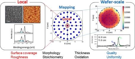
二维过渡金属二硫族化合物(TMDs)的晶圆级沉积是其在未来器件集成的关键。虽然已经做出了巨大的努力来提高二维材料的质量和均匀性,但它们的实施需要一个强大的表征方案来评估表面覆盖率、层数、化学计量、均匀性、结晶度和形态。在这项工作中,我们开发了一种结合局部分析和大规模方法的表征方案。该方案应用于使用两种不同前驱体通过原子层沉积(ALD)在SiO2衬底上生长的MoS2薄膜,从而确定了获得具有完整晶圆级覆盖的严格单层所需的ALD循环次数。原子力显微镜(AFM)、x射线光电子能谱(XPS)和扫描透射电子显微镜(STEM)提供了在低尺度下从亚单层到单层以上厚度范围内的成分、表面覆盖率和等效厚度的见解。波长色散x射线荧光(WDXRF)、扫描电子显微镜(SEM)、拉曼光谱和光致发光相结合,可以快速准确地评估晶圆尺度上的均匀性、晶圆上TMD薄膜的等效厚度和成分。
本文章由计算机程序翻译,如有差异,请以英文原文为准。

A wafer-scale method for the characterization of 2D MoS2 layers

A wafer-scale method for the characterization of 2D MoS2 layers
Wafer-scale deposition of 2D TMDs (Transition Metal Dichalcogenides) is a key point for their integration in future devices. While significant efforts have been dedicated to improving the quality and uniformity of 2D materials, their implementation requires a robust characterization protocol to assess the surface coverage, layer number, stoichiometry, homogeneity, crystallinity and morphology. In this work, we developed a characterization protocol that combined local analyses and large-scale methods. This protocol was applied to MoS2 films grown on SiO2 substrate by Atomic Layer Deposition (ALD) using two different precursors, enabling the determination of the number of ALD cycles required to achieve a strict monolayer with full wafer-scale coverage. Atomic Force Microscopy (AFM), X-ray Photoelectron Spectroscopy (XPS), and Scanning Transmission Electron Microscopy (STEM) provided insights into composition, surface coverage and equivalent thickness from sub-monolayer to above-monolayer thickness range at low scale. The combination of Wavelength-Dispersive X-ray Fluorescence (WDXRF), Scanning Electron Microscopy (SEM), Raman spectroscopy and Photoluminescence, enables a rapid and accurate evaluation of the uniformity at wafer scale, the equivalent thickness and composition of TMD films across the wafer.
求助全文
通过发布文献求助,成功后即可免费获取论文全文。 去求助
来源期刊
Applied Surface Science
Applied Surface Science 工程技术-材料科学:膜
CiteScore
12.50
自引率
7.50%
发文量
3393
审稿时长
67 days
期刊介绍: Applied Surface Science covers topics contributing to a better understanding of surfaces, interfaces, nanostructures and their applications. The journal is concerned with scientific research on the atomic and molecular level of material properties determined with specific surface analytical techniques and/or computational methods, as well as the processing of such structures.
×
引用
GB/T 7714-2015
复制
MLA
复制
APA
复制
导出至
BibTeX EndNote RefMan NoteFirst NoteExpress
×
提示
您的信息不完整,为了账户安全,请先补充。
现在去补充
×
提示
您因"违规操作"
具体请查看互助需知
我知道了
×
提示
确定
请完成安全验证×
copy
已复制链接
快去分享给好友吧!
我知道了
右上角分享
点击右上角分享
0
联系我们:info@booksci.cn Book学术提供免费学术资源搜索服务,方便国内外学者检索中英文文献。致力于提供最便捷和优质的服务体验。 Copyright © 2023 布克学术 All rights reserved.
京ICP备2023020795号-1
ghs 京公网安备 11010802042870号
Book学术文献互助
Book学术文献互助群
群 号:604180095
Book学术官方微信