{"title":"CBD合成WS2/p-Si异质结花瓣状薄膜的光敏性能","authors":"Avneesh Kumar, Ajeet Gupta, Surbhi, Himanshu Sharma, Munish Kumar Yadav, Anjali Verma, Mudit P. Srivastava, Devendra Kumar Rana","doi":"10.1007/s11664-025-12345-0","DOIUrl":null,"url":null,"abstract":"<div><p>Heterojunction WS<sub>2</sub>/p-Si thin film was synthesized using the chemical bath deposition (CBD) method. X-ray diffraction patterns show that the WS<sub>2</sub> thin film has high crystallinity with a hexagonal phase and crystallite size of ~221 nm. Field-emission scanning electron microscopy (FESEM) shows a petal-like morphology. The optical characteristics of the deposited WS<sub>2</sub> thin film were examined using ultraviolet–visible (UV–Vis) spectroscopy and photoluminescence (PL) spectroscopy, revealing an optical bandgap of approximately 2.33 eV in the visible spectrum. The PL emission spectrum shows multiple emission peaks between 400 nm and 675 nm. Current–voltage (<i>I–V</i>) characteristics were measured in the dark and at different light wavelengths, with the estimated ideality factor ranging from ~1.52 to ~1.67, which is very close to the ideal value for a diode. Current–time (<i>I–t</i>) measurement of the WS<sub>2</sub> thin film shows response and recovery time of ~0.01 s. The measurement at 5 V and forward biasing shows the lowest recovery and response time, which make it highly effective for detecting light in a broad range from the near-infrared to UV region.</p><h3>Graphical abstract</h3><div><figure><div><div><picture><source><img></source></picture></div></div></figure></div></div>","PeriodicalId":626,"journal":{"name":"Journal of Electronic Materials","volume":"54 11","pages":"9606 - 9618"},"PeriodicalIF":2.5000,"publicationDate":"2025-09-15","publicationTypes":"Journal Article","fieldsOfStudy":null,"isOpenAccess":false,"openAccessPdf":"","citationCount":"0","resultStr":"{\"title\":\"Light Sensing Properties of WS2/p-Si Heterojunction Petal-Like Morphology Thin Film Synthesized Using CBD\",\"authors\":\"Avneesh Kumar, Ajeet Gupta, Surbhi, Himanshu Sharma, Munish Kumar Yadav, Anjali Verma, Mudit P. Srivastava, Devendra Kumar Rana\",\"doi\":\"10.1007/s11664-025-12345-0\",\"DOIUrl\":null,\"url\":null,\"abstract\":\"<div><p>Heterojunction WS<sub>2</sub>/p-Si thin film was synthesized using the chemical bath deposition (CBD) method. X-ray diffraction patterns show that the WS<sub>2</sub> thin film has high crystallinity with a hexagonal phase and crystallite size of ~221 nm. Field-emission scanning electron microscopy (FESEM) shows a petal-like morphology. The optical characteristics of the deposited WS<sub>2</sub> thin film were examined using ultraviolet–visible (UV–Vis) spectroscopy and photoluminescence (PL) spectroscopy, revealing an optical bandgap of approximately 2.33 eV in the visible spectrum. The PL emission spectrum shows multiple emission peaks between 400 nm and 675 nm. Current–voltage (<i>I–V</i>) characteristics were measured in the dark and at different light wavelengths, with the estimated ideality factor ranging from ~1.52 to ~1.67, which is very close to the ideal value for a diode. Current–time (<i>I–t</i>) measurement of the WS<sub>2</sub> thin film shows response and recovery time of ~0.01 s. The measurement at 5 V and forward biasing shows the lowest recovery and response time, which make it highly effective for detecting light in a broad range from the near-infrared to UV region.</p><h3>Graphical abstract</h3><div><figure><div><div><picture><source><img></source></picture></div></div></figure></div></div>\",\"PeriodicalId\":626,\"journal\":{\"name\":\"Journal of Electronic Materials\",\"volume\":\"54 11\",\"pages\":\"9606 - 9618\"},\"PeriodicalIF\":2.5000,\"publicationDate\":\"2025-09-15\",\"publicationTypes\":\"Journal Article\",\"fieldsOfStudy\":null,\"isOpenAccess\":false,\"openAccessPdf\":\"\",\"citationCount\":\"0\",\"resultStr\":null,\"platform\":\"Semanticscholar\",\"paperid\":null,\"PeriodicalName\":\"Journal of Electronic Materials\",\"FirstCategoryId\":\"5\",\"ListUrlMain\":\"https://link.springer.com/article/10.1007/s11664-025-12345-0\",\"RegionNum\":4,\"RegionCategory\":\"工程技术\",\"ArticlePicture\":[],\"TitleCN\":null,\"AbstractTextCN\":null,\"PMCID\":null,\"EPubDate\":\"\",\"PubModel\":\"\",\"JCR\":\"Q3\",\"JCRName\":\"ENGINEERING, ELECTRICAL & ELECTRONIC\",\"Score\":null,\"Total\":0}","platform":"Semanticscholar","paperid":null,"PeriodicalName":"Journal of Electronic Materials","FirstCategoryId":"5","ListUrlMain":"https://link.springer.com/article/10.1007/s11664-025-12345-0","RegionNum":4,"RegionCategory":"工程技术","ArticlePicture":[],"TitleCN":null,"AbstractTextCN":null,"PMCID":null,"EPubDate":"","PubModel":"","JCR":"Q3","JCRName":"ENGINEERING, ELECTRICAL & ELECTRONIC","Score":null,"Total":0}
Light Sensing Properties of WS2/p-Si Heterojunction Petal-Like Morphology Thin Film Synthesized Using CBD
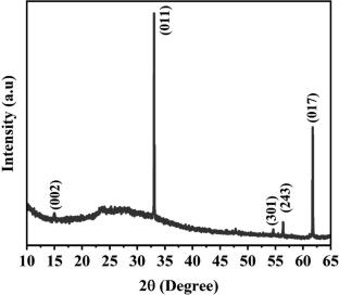
Heterojunction WS2/p-Si thin film was synthesized using the chemical bath deposition (CBD) method. X-ray diffraction patterns show that the WS2 thin film has high crystallinity with a hexagonal phase and crystallite size of ~221 nm. Field-emission scanning electron microscopy (FESEM) shows a petal-like morphology. The optical characteristics of the deposited WS2 thin film were examined using ultraviolet–visible (UV–Vis) spectroscopy and photoluminescence (PL) spectroscopy, revealing an optical bandgap of approximately 2.33 eV in the visible spectrum. The PL emission spectrum shows multiple emission peaks between 400 nm and 675 nm. Current–voltage (I–V) characteristics were measured in the dark and at different light wavelengths, with the estimated ideality factor ranging from ~1.52 to ~1.67, which is very close to the ideal value for a diode. Current–time (I–t) measurement of the WS2 thin film shows response and recovery time of ~0.01 s. The measurement at 5 V and forward biasing shows the lowest recovery and response time, which make it highly effective for detecting light in a broad range from the near-infrared to UV region.
期刊介绍:
The Journal of Electronic Materials (JEM) reports monthly on the science and technology of electronic materials, while examining new applications for semiconductors, magnetic alloys, dielectrics, nanoscale materials, and photonic materials. The journal welcomes articles on methods for preparing and evaluating the chemical, physical, electronic, and optical properties of these materials. Specific areas of interest are materials for state-of-the-art transistors, nanotechnology, electronic packaging, detectors, emitters, metallization, superconductivity, and energy applications.
Review papers on current topics enable individuals in the field of electronics to keep abreast of activities in areas peripheral to their own. JEM also selects papers from conferences such as the Electronic Materials Conference, the U.S. Workshop on the Physics and Chemistry of II-VI Materials, and the International Conference on Thermoelectrics. It benefits both specialists and non-specialists in the electronic materials field.
A journal of The Minerals, Metals & Materials Society.
 求助内容:
求助内容: 应助结果提醒方式:


