M. Yasir Ali, Ausaf Ahmed, A. Ali, Azhar Mehmood, M. Sharafat Hussain, Chun-Ming Wang, K. Mahmood
{"title":"FeSi2合金生长后退火获得花状表面形貌的功率因数优化","authors":"M. Yasir Ali, Ausaf Ahmed, A. Ali, Azhar Mehmood, M. Sharafat Hussain, Chun-Ming Wang, K. Mahmood","doi":"10.1007/s11664-025-12312-9","DOIUrl":null,"url":null,"abstract":"<div><p>In this work, we have successfully optimized the power factor value for an FeSi<sub>2</sub> alloy by achieving a flower-like surface morphology. The samples used in this study were prepared using a solid-state reaction method. Fe and Si powders were mixed in a weight ratio of 2:1, and pellets were formed using a high-pressure press. The pellets were annealed at different temperatures in the range of 500–1000°C for 1 h using an air muffle furnace. X-ray diffraction (XRD) data confirmed the tetragonal lattice structure of all samples, and it was further evident that the crystal structure degraded as the annealing temperature increased to 900°C and 1000°C. A very high Seebeck coefficient (470 µV/K) was achieved for the sample annealed at 1000°C due to the emergence of a flower-like surface morphology with high-temperature annealing, as verified by scanning electron microscopy (SEM) images. On the other hand, electrical conductivity data suggested a decreasing trend with annealing temperature, because oxide-based insulating phases developed at a high annealing temperature due to the involvement of oxygen during the annealing process. However, the decreasing trend in electrical conductivity is not as great as the increasing behaviour of the Seebeck coefficient. Therefore, an optimized power factor value (3.5 × 10<sup>−5</sup> W/m·K<sup>2</sup>) was achieved at the optimal annealing temperature of 700°C.</p></div>","PeriodicalId":626,"journal":{"name":"Journal of Electronic Materials","volume":"54 11","pages":"9695 - 9699"},"PeriodicalIF":2.5000,"publicationDate":"2025-09-05","publicationTypes":"Journal Article","fieldsOfStudy":null,"isOpenAccess":false,"openAccessPdf":"","citationCount":"0","resultStr":"{\"title\":\"Optimizing the Power Factor of FeSi2 Alloy by Achieving Flower-Like Surface Morphology Using Post-Growth Annealing\",\"authors\":\"M. Yasir Ali, Ausaf Ahmed, A. Ali, Azhar Mehmood, M. Sharafat Hussain, Chun-Ming Wang, K. Mahmood\",\"doi\":\"10.1007/s11664-025-12312-9\",\"DOIUrl\":null,\"url\":null,\"abstract\":\"<div><p>In this work, we have successfully optimized the power factor value for an FeSi<sub>2</sub> alloy by achieving a flower-like surface morphology. The samples used in this study were prepared using a solid-state reaction method. Fe and Si powders were mixed in a weight ratio of 2:1, and pellets were formed using a high-pressure press. The pellets were annealed at different temperatures in the range of 500–1000°C for 1 h using an air muffle furnace. X-ray diffraction (XRD) data confirmed the tetragonal lattice structure of all samples, and it was further evident that the crystal structure degraded as the annealing temperature increased to 900°C and 1000°C. A very high Seebeck coefficient (470 µV/K) was achieved for the sample annealed at 1000°C due to the emergence of a flower-like surface morphology with high-temperature annealing, as verified by scanning electron microscopy (SEM) images. On the other hand, electrical conductivity data suggested a decreasing trend with annealing temperature, because oxide-based insulating phases developed at a high annealing temperature due to the involvement of oxygen during the annealing process. However, the decreasing trend in electrical conductivity is not as great as the increasing behaviour of the Seebeck coefficient. Therefore, an optimized power factor value (3.5 × 10<sup>−5</sup> W/m·K<sup>2</sup>) was achieved at the optimal annealing temperature of 700°C.</p></div>\",\"PeriodicalId\":626,\"journal\":{\"name\":\"Journal of Electronic Materials\",\"volume\":\"54 11\",\"pages\":\"9695 - 9699\"},\"PeriodicalIF\":2.5000,\"publicationDate\":\"2025-09-05\",\"publicationTypes\":\"Journal Article\",\"fieldsOfStudy\":null,\"isOpenAccess\":false,\"openAccessPdf\":\"\",\"citationCount\":\"0\",\"resultStr\":null,\"platform\":\"Semanticscholar\",\"paperid\":null,\"PeriodicalName\":\"Journal of Electronic Materials\",\"FirstCategoryId\":\"5\",\"ListUrlMain\":\"https://link.springer.com/article/10.1007/s11664-025-12312-9\",\"RegionNum\":4,\"RegionCategory\":\"工程技术\",\"ArticlePicture\":[],\"TitleCN\":null,\"AbstractTextCN\":null,\"PMCID\":null,\"EPubDate\":\"\",\"PubModel\":\"\",\"JCR\":\"Q3\",\"JCRName\":\"ENGINEERING, ELECTRICAL & ELECTRONIC\",\"Score\":null,\"Total\":0}","platform":"Semanticscholar","paperid":null,"PeriodicalName":"Journal of Electronic Materials","FirstCategoryId":"5","ListUrlMain":"https://link.springer.com/article/10.1007/s11664-025-12312-9","RegionNum":4,"RegionCategory":"工程技术","ArticlePicture":[],"TitleCN":null,"AbstractTextCN":null,"PMCID":null,"EPubDate":"","PubModel":"","JCR":"Q3","JCRName":"ENGINEERING, ELECTRICAL & ELECTRONIC","Score":null,"Total":0}
Optimizing the Power Factor of FeSi2 Alloy by Achieving Flower-Like Surface Morphology Using Post-Growth Annealing
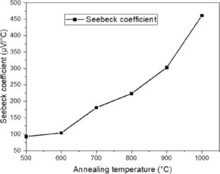
In this work, we have successfully optimized the power factor value for an FeSi2 alloy by achieving a flower-like surface morphology. The samples used in this study were prepared using a solid-state reaction method. Fe and Si powders were mixed in a weight ratio of 2:1, and pellets were formed using a high-pressure press. The pellets were annealed at different temperatures in the range of 500–1000°C for 1 h using an air muffle furnace. X-ray diffraction (XRD) data confirmed the tetragonal lattice structure of all samples, and it was further evident that the crystal structure degraded as the annealing temperature increased to 900°C and 1000°C. A very high Seebeck coefficient (470 µV/K) was achieved for the sample annealed at 1000°C due to the emergence of a flower-like surface morphology with high-temperature annealing, as verified by scanning electron microscopy (SEM) images. On the other hand, electrical conductivity data suggested a decreasing trend with annealing temperature, because oxide-based insulating phases developed at a high annealing temperature due to the involvement of oxygen during the annealing process. However, the decreasing trend in electrical conductivity is not as great as the increasing behaviour of the Seebeck coefficient. Therefore, an optimized power factor value (3.5 × 10⁻⁵ W/m·K2) was achieved at the optimal annealing temperature of 700°C.
期刊介绍:
The Journal of Electronic Materials (JEM) reports monthly on the science and technology of electronic materials, while examining new applications for semiconductors, magnetic alloys, dielectrics, nanoscale materials, and photonic materials. The journal welcomes articles on methods for preparing and evaluating the chemical, physical, electronic, and optical properties of these materials. Specific areas of interest are materials for state-of-the-art transistors, nanotechnology, electronic packaging, detectors, emitters, metallization, superconductivity, and energy applications.
Review papers on current topics enable individuals in the field of electronics to keep abreast of activities in areas peripheral to their own. JEM also selects papers from conferences such as the Electronic Materials Conference, the U.S. Workshop on the Physics and Chemistry of II-VI Materials, and the International Conference on Thermoelectrics. It benefits both specialists and non-specialists in the electronic materials field.
A journal of The Minerals, Metals & Materials Society.
 求助内容:
求助内容: 应助结果提醒方式:


