Mingyu Jung, , , Alan Jiwan Yun, , , Yuhyeon Oh, , , Shashank Shekhar, , , Byungwoo Park, , and , Seunghun Hong*,
{"title":"基于波长相关噪声显微镜的钙钛矿太阳能电池结构中电荷阱诱导的局域带隙变化的纳米尺度映射","authors":"Mingyu Jung, , , Alan Jiwan Yun, , , Yuhyeon Oh, , , Shashank Shekhar, , , Byungwoo Park, , and , Seunghun Hong*, ","doi":"10.1021/acsami.5c15108","DOIUrl":null,"url":null,"abstract":"<p >We report the nanoscale mapping of charge-trap-induced local bandgap variations in an organic–inorganic halide perovskite film within a solar cell structure. For mapping, a conducting probe scanned the perovskite film surface under monochromatic illumination at different wavelengths to simultaneously map wavelength-dependent photocurrents and electrical noise. The measured maps were analyzed further to obtain the spatial distributions of photoconductive properties, such as photocurrent (<i>I</i><sub>pc</sub>), short-circuit current (<i>I</i><sub>sc</sub>), and charge trap density (<i>N</i><sub>eff</sub>), in the film. Interestingly, both the photocurrent and short-circuit current exhibited negative correlations with trap density following distinct power-law relationships. Importantly, a local bandgap (<i>E</i><sub>g</sub>) map was obtained from wavelength-dependent photocurrent maps by applying the Tauc plot method with local external quantum efficiencies (<i>EQE</i>) at different wavelengths, revealing spatial variations across the perovskite film. Quantitative analysis revealed a correlation between variations of bandgap and effective trap density following Δ<i>E</i><sub>g</sub> ∝ <i>N</i><sub>eff</sub><i><sup>–</sup></i><sup>0.01</sup>, indicating that localized traps near the band edges effectively reduce the bandgaps. Our strategy enables direct mapping of nanoscale photoconductive properties and their quantitative correlations, providing a powerful tool for both fundamental research and practical applications in optoelectronic devices.</p>","PeriodicalId":5,"journal":{"name":"ACS Applied Materials & Interfaces","volume":"17 41","pages":"57133–57141"},"PeriodicalIF":8.2000,"publicationDate":"2025-10-06","publicationTypes":"Journal Article","fieldsOfStudy":null,"isOpenAccess":false,"openAccessPdf":"","citationCount":"0","resultStr":"{\"title\":\"Nanoscale Mapping of Charge-Trap-Induced Localized Bandgap Variations in Perovskite Solar Cell Structures via Wavelength-Dependent Noise Microscopy\",\"authors\":\"Mingyu Jung, , , Alan Jiwan Yun, , , Yuhyeon Oh, , , Shashank Shekhar, , , Byungwoo Park, , and , Seunghun Hong*, \",\"doi\":\"10.1021/acsami.5c15108\",\"DOIUrl\":null,\"url\":null,\"abstract\":\"<p >We report the nanoscale mapping of charge-trap-induced local bandgap variations in an organic–inorganic halide perovskite film within a solar cell structure. For mapping, a conducting probe scanned the perovskite film surface under monochromatic illumination at different wavelengths to simultaneously map wavelength-dependent photocurrents and electrical noise. The measured maps were analyzed further to obtain the spatial distributions of photoconductive properties, such as photocurrent (<i>I</i><sub>pc</sub>), short-circuit current (<i>I</i><sub>sc</sub>), and charge trap density (<i>N</i><sub>eff</sub>), in the film. Interestingly, both the photocurrent and short-circuit current exhibited negative correlations with trap density following distinct power-law relationships. Importantly, a local bandgap (<i>E</i><sub>g</sub>) map was obtained from wavelength-dependent photocurrent maps by applying the Tauc plot method with local external quantum efficiencies (<i>EQE</i>) at different wavelengths, revealing spatial variations across the perovskite film. Quantitative analysis revealed a correlation between variations of bandgap and effective trap density following Δ<i>E</i><sub>g</sub> ∝ <i>N</i><sub>eff</sub><i><sup>–</sup></i><sup>0.01</sup>, indicating that localized traps near the band edges effectively reduce the bandgaps. Our strategy enables direct mapping of nanoscale photoconductive properties and their quantitative correlations, providing a powerful tool for both fundamental research and practical applications in optoelectronic devices.</p>\",\"PeriodicalId\":5,\"journal\":{\"name\":\"ACS Applied Materials & Interfaces\",\"volume\":\"17 41\",\"pages\":\"57133–57141\"},\"PeriodicalIF\":8.2000,\"publicationDate\":\"2025-10-06\",\"publicationTypes\":\"Journal Article\",\"fieldsOfStudy\":null,\"isOpenAccess\":false,\"openAccessPdf\":\"\",\"citationCount\":\"0\",\"resultStr\":null,\"platform\":\"Semanticscholar\",\"paperid\":null,\"PeriodicalName\":\"ACS Applied Materials & Interfaces\",\"FirstCategoryId\":\"88\",\"ListUrlMain\":\"https://pubs.acs.org/doi/10.1021/acsami.5c15108\",\"RegionNum\":2,\"RegionCategory\":\"材料科学\",\"ArticlePicture\":[],\"TitleCN\":null,\"AbstractTextCN\":null,\"PMCID\":null,\"EPubDate\":\"\",\"PubModel\":\"\",\"JCR\":\"Q1\",\"JCRName\":\"MATERIALS SCIENCE, MULTIDISCIPLINARY\",\"Score\":null,\"Total\":0}","platform":"Semanticscholar","paperid":null,"PeriodicalName":"ACS Applied Materials & Interfaces","FirstCategoryId":"88","ListUrlMain":"https://pubs.acs.org/doi/10.1021/acsami.5c15108","RegionNum":2,"RegionCategory":"材料科学","ArticlePicture":[],"TitleCN":null,"AbstractTextCN":null,"PMCID":null,"EPubDate":"","PubModel":"","JCR":"Q1","JCRName":"MATERIALS SCIENCE, MULTIDISCIPLINARY","Score":null,"Total":0}
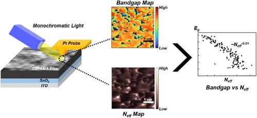
Nanoscale Mapping of Charge-Trap-Induced Localized Bandgap Variations in Perovskite Solar Cell Structures via Wavelength-Dependent Noise Microscopy
We report the nanoscale mapping of charge-trap-induced local bandgap variations in an organic–inorganic halide perovskite film within a solar cell structure. For mapping, a conducting probe scanned the perovskite film surface under monochromatic illumination at different wavelengths to simultaneously map wavelength-dependent photocurrents and electrical noise. The measured maps were analyzed further to obtain the spatial distributions of photoconductive properties, such as photocurrent (Ipc), short-circuit current (Isc), and charge trap density (Neff), in the film. Interestingly, both the photocurrent and short-circuit current exhibited negative correlations with trap density following distinct power-law relationships. Importantly, a local bandgap (Eg) map was obtained from wavelength-dependent photocurrent maps by applying the Tauc plot method with local external quantum efficiencies (EQE) at different wavelengths, revealing spatial variations across the perovskite film. Quantitative analysis revealed a correlation between variations of bandgap and effective trap density following ΔEg ∝ Neff–0.01, indicating that localized traps near the band edges effectively reduce the bandgaps. Our strategy enables direct mapping of nanoscale photoconductive properties and their quantitative correlations, providing a powerful tool for both fundamental research and practical applications in optoelectronic devices.
期刊介绍:
ACS Applied Materials & Interfaces is a leading interdisciplinary journal that brings together chemists, engineers, physicists, and biologists to explore the development and utilization of newly-discovered materials and interfacial processes for specific applications. Our journal has experienced remarkable growth since its establishment in 2009, both in terms of the number of articles published and the impact of the research showcased. We are proud to foster a truly global community, with the majority of published articles originating from outside the United States, reflecting the rapid growth of applied research worldwide.


 求助内容:
求助内容: 应助结果提醒方式:


