一种具有异质结和缓冲层的新型双沟栅4H-SiC LDMOS,可提高单事件烧蚀耐受性

IF 1.9 3区 工程技术 Q3 ENGINEERING, ELECTRICAL & ELECTRONIC
Liqun Wang, Panpan Tang, Tong Liu
{"title":"一种具有异质结和缓冲层的新型双沟栅4H-SiC LDMOS,可提高单事件烧蚀耐受性","authors":"Liqun Wang,&nbsp;Panpan Tang,&nbsp;Tong Liu","doi":"10.1016/j.mejo.2025.106909","DOIUrl":null,"url":null,"abstract":"<div><div>As an important aerospace power device, silicon carbide (SiC) Lateral Diffused Metal Oxide Semiconductor (LDMOS) is susceptible to single-event burnout (SEB), which causes catastrophic damage when exposed to space radiation. The current work employs the Sentaurus TCAD simulations to present the SEB hardening method for a 1.2-kV 4H-SiC LDMOS. A double-trench gate 4H-SiC LDMOS containing low specific on-resistance (<span><math><msub><mrow><mi>R</mi></mrow><mrow><mi>o</mi><mi>n</mi><mo>,</mo><mi>s</mi><mi>p</mi></mrow></msub></math></span>) is proposed, significantly improving the device’s SEB threshold voltage (<span><math><msub><mrow><mi>V</mi></mrow><mrow><mi>S</mi><mi>E</mi><mi>B</mi></mrow></msub></math></span>). The proposed hardening design integrates multi-buffer layer with a heterojunction, impressively mitigating the high electric field at the drain area while suppressing the parasitic bipolar junction transistor (BJT). Besides, the device’s resistance is significantly decreased by designing the double-trench gate and current spreading layer (CSL). Accordingly, the constructed device achieves a (498 ± 11)% increase in <span><math><msub><mrow><mi>V</mi></mrow><mrow><mi>S</mi><mi>E</mi><mi>B</mi></mrow></msub></math></span> while reducing the <span><math><msub><mrow><mi>R</mi></mrow><mrow><mi>o</mi><mi>n</mi><mo>,</mo><mi>s</mi><mi>p</mi></mrow></msub></math></span> by (41.8 ± 1.8)% compared with the traditional 4H-SiC LDMOS. This significantly enhances the device’s reliability in radiation environments.</div></div>","PeriodicalId":49818,"journal":{"name":"Microelectronics Journal","volume":"166 ","pages":"Article 106909"},"PeriodicalIF":1.9000,"publicationDate":"2025-09-27","publicationTypes":"Journal Article","fieldsOfStudy":null,"isOpenAccess":false,"openAccessPdf":"","citationCount":"0","resultStr":"{\"title\":\"A new double-trench gate 4H-SiC LDMOS with heterojunction and buffer layer for improved single-event burnout tolerance\",\"authors\":\"Liqun Wang,&nbsp;Panpan Tang,&nbsp;Tong Liu\",\"doi\":\"10.1016/j.mejo.2025.106909\",\"DOIUrl\":null,\"url\":null,\"abstract\":\"<div><div>As an important aerospace power device, silicon carbide (SiC) Lateral Diffused Metal Oxide Semiconductor (LDMOS) is susceptible to single-event burnout (SEB), which causes catastrophic damage when exposed to space radiation. The current work employs the Sentaurus TCAD simulations to present the SEB hardening method for a 1.2-kV 4H-SiC LDMOS. A double-trench gate 4H-SiC LDMOS containing low specific on-resistance (<span><math><msub><mrow><mi>R</mi></mrow><mrow><mi>o</mi><mi>n</mi><mo>,</mo><mi>s</mi><mi>p</mi></mrow></msub></math></span>) is proposed, significantly improving the device’s SEB threshold voltage (<span><math><msub><mrow><mi>V</mi></mrow><mrow><mi>S</mi><mi>E</mi><mi>B</mi></mrow></msub></math></span>). The proposed hardening design integrates multi-buffer layer with a heterojunction, impressively mitigating the high electric field at the drain area while suppressing the parasitic bipolar junction transistor (BJT). Besides, the device’s resistance is significantly decreased by designing the double-trench gate and current spreading layer (CSL). Accordingly, the constructed device achieves a (498 ± 11)% increase in <span><math><msub><mrow><mi>V</mi></mrow><mrow><mi>S</mi><mi>E</mi><mi>B</mi></mrow></msub></math></span> while reducing the <span><math><msub><mrow><mi>R</mi></mrow><mrow><mi>o</mi><mi>n</mi><mo>,</mo><mi>s</mi><mi>p</mi></mrow></msub></math></span> by (41.8 ± 1.8)% compared with the traditional 4H-SiC LDMOS. This significantly enhances the device’s reliability in radiation environments.</div></div>\",\"PeriodicalId\":49818,\"journal\":{\"name\":\"Microelectronics Journal\",\"volume\":\"166 \",\"pages\":\"Article 106909\"},\"PeriodicalIF\":1.9000,\"publicationDate\":\"2025-09-27\",\"publicationTypes\":\"Journal Article\",\"fieldsOfStudy\":null,\"isOpenAccess\":false,\"openAccessPdf\":\"\",\"citationCount\":\"0\",\"resultStr\":null,\"platform\":\"Semanticscholar\",\"paperid\":null,\"PeriodicalName\":\"Microelectronics Journal\",\"FirstCategoryId\":\"5\",\"ListUrlMain\":\"https://www.sciencedirect.com/science/article/pii/S1879239125003583\",\"RegionNum\":3,\"RegionCategory\":\"工程技术\",\"ArticlePicture\":[],\"TitleCN\":null,\"AbstractTextCN\":null,\"PMCID\":null,\"EPubDate\":\"\",\"PubModel\":\"\",\"JCR\":\"Q3\",\"JCRName\":\"ENGINEERING, ELECTRICAL & ELECTRONIC\",\"Score\":null,\"Total\":0}","platform":"Semanticscholar","paperid":null,"PeriodicalName":"Microelectronics Journal","FirstCategoryId":"5","ListUrlMain":"https://www.sciencedirect.com/science/article/pii/S1879239125003583","RegionNum":3,"RegionCategory":"工程技术","ArticlePicture":[],"TitleCN":null,"AbstractTextCN":null,"PMCID":null,"EPubDate":"","PubModel":"","JCR":"Q3","JCRName":"ENGINEERING, ELECTRICAL & ELECTRONIC","Score":null,"Total":0}
引用次数: 0

摘要

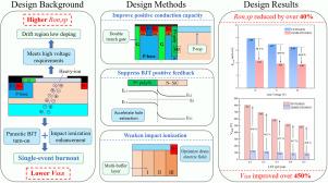
作为重要的航天动力器件,碳化硅(SiC)横向扩散金属氧化物半导体(LDMOS)暴露在空间辐射下容易发生单事件烧坏(SEB),造成灾难性的破坏。本文采用Sentaurus TCAD模拟,提出了1.2 kv 4H-SiC LDMOS的SEB硬化方法。提出了一种低比导通电阻(Ron,sp)的双沟槽栅极4H-SiC LDMOS,显著提高了器件的SEB阈值电压(VSEB)。提出的硬化设计集成了多缓冲层和异质结,令人印象深刻地减轻了漏极区域的高电场,同时抑制了寄生双极结晶体管(BJT)。此外,通过设计双沟槽栅极和扩流层(CSL),器件电阻显著降低。因此,与传统的4H-SiC LDMOS相比,该器件的VSEB提高了(498±11)%,而Ron,sp降低了(41.8±1.8)%。这大大提高了器件在辐射环境中的可靠性。
本文章由计算机程序翻译,如有差异,请以英文原文为准。

A new double-trench gate 4H-SiC LDMOS with heterojunction and buffer layer for improved single-event burnout tolerance

A new double-trench gate 4H-SiC LDMOS with heterojunction and buffer layer for improved single-event burnout tolerance
As an important aerospace power device, silicon carbide (SiC) Lateral Diffused Metal Oxide Semiconductor (LDMOS) is susceptible to single-event burnout (SEB), which causes catastrophic damage when exposed to space radiation. The current work employs the Sentaurus TCAD simulations to present the SEB hardening method for a 1.2-kV 4H-SiC LDMOS. A double-trench gate 4H-SiC LDMOS containing low specific on-resistance (Ron,sp) is proposed, significantly improving the device’s SEB threshold voltage (VSEB). The proposed hardening design integrates multi-buffer layer with a heterojunction, impressively mitigating the high electric field at the drain area while suppressing the parasitic bipolar junction transistor (BJT). Besides, the device’s resistance is significantly decreased by designing the double-trench gate and current spreading layer (CSL). Accordingly, the constructed device achieves a (498 ± 11)% increase in VSEB while reducing the Ron,sp by (41.8 ± 1.8)% compared with the traditional 4H-SiC LDMOS. This significantly enhances the device’s reliability in radiation environments.
求助全文
通过发布文献求助,成功后即可免费获取论文全文。 去求助
来源期刊
Microelectronics Journal
Microelectronics Journal 工程技术-工程:电子与电气
CiteScore
4.00
自引率
27.30%
发文量
222
审稿时长
43 days
期刊介绍: Published since 1969, the Microelectronics Journal is an international forum for the dissemination of research and applications of microelectronic systems, circuits, and emerging technologies. Papers published in the Microelectronics Journal have undergone peer review to ensure originality, relevance, and timeliness. The journal thus provides a worldwide, regular, and comprehensive update on microelectronic circuits and systems. The Microelectronics Journal invites papers describing significant research and applications in all of the areas listed below. Comprehensive review/survey papers covering recent developments will also be considered. The Microelectronics Journal covers circuits and systems. This topic includes but is not limited to: Analog, digital, mixed, and RF circuits and related design methodologies; Logic, architectural, and system level synthesis; Testing, design for testability, built-in self-test; Area, power, and thermal analysis and design; Mixed-domain simulation and design; Embedded systems; Non-von Neumann computing and related technologies and circuits; Design and test of high complexity systems integration; SoC, NoC, SIP, and NIP design and test; 3-D integration design and analysis; Emerging device technologies and circuits, such as FinFETs, SETs, spintronics, SFQ, MTJ, etc. Application aspects such as signal and image processing including circuits for cryptography, sensors, and actuators including sensor networks, reliability and quality issues, and economic models are also welcome.
×
引用
GB/T 7714-2015
复制
MLA
复制
APA
复制
导出至
BibTeX EndNote RefMan NoteFirst NoteExpress
×
提示
您的信息不完整,为了账户安全,请先补充。
现在去补充
×
提示
您因"违规操作"
具体请查看互助需知
我知道了
×
提示
确定
请完成安全验证×
copy
已复制链接
快去分享给好友吧!
我知道了
右上角分享
点击右上角分享
0
联系我们:info@booksci.cn Book学术提供免费学术资源搜索服务,方便国内外学者检索中英文文献。致力于提供最便捷和优质的服务体验。 Copyright © 2023 布克学术 All rights reserved.
京ICP备2023020795号-1
ghs 京公网安备 11010802042870号
Book学术文献互助
Book学术文献互助群
群 号:604180095
Book学术官方微信