{"title":"原子薄半导体激子动力学相变工程","authors":"Sihan Lin, , , Zeliang Zhang, , , Wenqi Qian, , , Haiyi Liu, , , Tengteng Gao, , , Changlin Sun, , , Guangyi Tao, , , Fangxun Liu, , , Lie Lin, , , Pengfei Qi*, , , Li-Guo Zhu, , , Zheyu Fang, , and , Weiwei Liu, ","doi":"10.1021/acsphotonics.5c01269","DOIUrl":null,"url":null,"abstract":"<p >Two-dimensional excitonic devices are of great potential to overcome the dilemma of response time and integration in current electronic and/or photonic systems, where dynamically controlling the spatiotemporal dynamics of exciton flux is a cornerstone. Although tip-induced strain engineering and surface acoustic waves (SAWs) have been proposed, the complex accessorial configurations severely limit the applications in integrated devices. Here, we systematically investigate phase transition engineering of vanadium dioxide (VO<sub>2</sub>) for exciton dynamics in an atomically thin semiconductor. Temperature-dependent photoluminescence (PL) spectra demonstrate that PL reaches a maximum at the phase transition temperature <i>T</i><sub>c</sub> (340 K), due to the increase in free carrier density during the insulator-to-metal transition. The thermal hysteresis loop is first observed from PL spectra due to the latent heat in the phase transition. The increased free carrier density during the VO<sub>2</sub> phase transition can dynamically modulate the exciton diffusion coefficient, where the enhanced charged excitons (trions) near the insulator–metal transition temperature promote the exciton diffusion coefficient. The hexagonal boron nitride (hBN) intercalation mitigates the VO<sub>2</sub>-induced negative effects through dielectric screening and interfacial defect reduction while preserving the dynamic phase transition modulation capability in the PL spectra and yielding a more than doubled enhancement of the exciton diffusion coefficient. These findings highlight the importance of phase transition engineering for two-dimensional (2D) exciton-based devices and lay a foundation for the development of functional excitonic devices.</p>","PeriodicalId":23,"journal":{"name":"ACS Photonics","volume":"12 10","pages":"5537–5547"},"PeriodicalIF":6.7000,"publicationDate":"2025-09-30","publicationTypes":"Journal Article","fieldsOfStudy":null,"isOpenAccess":false,"openAccessPdf":"","citationCount":"0","resultStr":"{\"title\":\"Phase Transition Engineering for Exciton Dynamics in Atomically Thin Semiconductors\",\"authors\":\"Sihan Lin, , , Zeliang Zhang, , , Wenqi Qian, , , Haiyi Liu, , , Tengteng Gao, , , Changlin Sun, , , Guangyi Tao, , , Fangxun Liu, , , Lie Lin, , , Pengfei Qi*, , , Li-Guo Zhu, , , Zheyu Fang, , and , Weiwei Liu, \",\"doi\":\"10.1021/acsphotonics.5c01269\",\"DOIUrl\":null,\"url\":null,\"abstract\":\"<p >Two-dimensional excitonic devices are of great potential to overcome the dilemma of response time and integration in current electronic and/or photonic systems, where dynamically controlling the spatiotemporal dynamics of exciton flux is a cornerstone. Although tip-induced strain engineering and surface acoustic waves (SAWs) have been proposed, the complex accessorial configurations severely limit the applications in integrated devices. Here, we systematically investigate phase transition engineering of vanadium dioxide (VO<sub>2</sub>) for exciton dynamics in an atomically thin semiconductor. Temperature-dependent photoluminescence (PL) spectra demonstrate that PL reaches a maximum at the phase transition temperature <i>T</i><sub>c</sub> (340 K), due to the increase in free carrier density during the insulator-to-metal transition. The thermal hysteresis loop is first observed from PL spectra due to the latent heat in the phase transition. The increased free carrier density during the VO<sub>2</sub> phase transition can dynamically modulate the exciton diffusion coefficient, where the enhanced charged excitons (trions) near the insulator–metal transition temperature promote the exciton diffusion coefficient. The hexagonal boron nitride (hBN) intercalation mitigates the VO<sub>2</sub>-induced negative effects through dielectric screening and interfacial defect reduction while preserving the dynamic phase transition modulation capability in the PL spectra and yielding a more than doubled enhancement of the exciton diffusion coefficient. These findings highlight the importance of phase transition engineering for two-dimensional (2D) exciton-based devices and lay a foundation for the development of functional excitonic devices.</p>\",\"PeriodicalId\":23,\"journal\":{\"name\":\"ACS Photonics\",\"volume\":\"12 10\",\"pages\":\"5537–5547\"},\"PeriodicalIF\":6.7000,\"publicationDate\":\"2025-09-30\",\"publicationTypes\":\"Journal Article\",\"fieldsOfStudy\":null,\"isOpenAccess\":false,\"openAccessPdf\":\"\",\"citationCount\":\"0\",\"resultStr\":null,\"platform\":\"Semanticscholar\",\"paperid\":null,\"PeriodicalName\":\"ACS Photonics\",\"FirstCategoryId\":\"101\",\"ListUrlMain\":\"https://pubs.acs.org/doi/10.1021/acsphotonics.5c01269\",\"RegionNum\":1,\"RegionCategory\":\"物理与天体物理\",\"ArticlePicture\":[],\"TitleCN\":null,\"AbstractTextCN\":null,\"PMCID\":null,\"EPubDate\":\"\",\"PubModel\":\"\",\"JCR\":\"Q1\",\"JCRName\":\"MATERIALS SCIENCE, MULTIDISCIPLINARY\",\"Score\":null,\"Total\":0}","platform":"Semanticscholar","paperid":null,"PeriodicalName":"ACS Photonics","FirstCategoryId":"101","ListUrlMain":"https://pubs.acs.org/doi/10.1021/acsphotonics.5c01269","RegionNum":1,"RegionCategory":"物理与天体物理","ArticlePicture":[],"TitleCN":null,"AbstractTextCN":null,"PMCID":null,"EPubDate":"","PubModel":"","JCR":"Q1","JCRName":"MATERIALS SCIENCE, MULTIDISCIPLINARY","Score":null,"Total":0}
Phase Transition Engineering for Exciton Dynamics in Atomically Thin Semiconductors
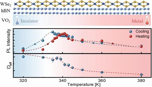
Two-dimensional excitonic devices are of great potential to overcome the dilemma of response time and integration in current electronic and/or photonic systems, where dynamically controlling the spatiotemporal dynamics of exciton flux is a cornerstone. Although tip-induced strain engineering and surface acoustic waves (SAWs) have been proposed, the complex accessorial configurations severely limit the applications in integrated devices. Here, we systematically investigate phase transition engineering of vanadium dioxide (VO2) for exciton dynamics in an atomically thin semiconductor. Temperature-dependent photoluminescence (PL) spectra demonstrate that PL reaches a maximum at the phase transition temperature Tc (340 K), due to the increase in free carrier density during the insulator-to-metal transition. The thermal hysteresis loop is first observed from PL spectra due to the latent heat in the phase transition. The increased free carrier density during the VO2 phase transition can dynamically modulate the exciton diffusion coefficient, where the enhanced charged excitons (trions) near the insulator–metal transition temperature promote the exciton diffusion coefficient. The hexagonal boron nitride (hBN) intercalation mitigates the VO2-induced negative effects through dielectric screening and interfacial defect reduction while preserving the dynamic phase transition modulation capability in the PL spectra and yielding a more than doubled enhancement of the exciton diffusion coefficient. These findings highlight the importance of phase transition engineering for two-dimensional (2D) exciton-based devices and lay a foundation for the development of functional excitonic devices.
期刊介绍:
Published as soon as accepted and summarized in monthly issues, ACS Photonics will publish Research Articles, Letters, Perspectives, and Reviews, to encompass the full scope of published research in this field.


 求助内容:
求助内容: 应助结果提醒方式:


