Yong Zhang, , , Kevin Chang, , , Huilong Yan, , , Chi-Hsin Huang, , and , Kenji Nomura*,
{"title":"非晶氧化镓光电晶体管在光学传感器神经形态中的应用。","authors":"Yong Zhang, , , Kevin Chang, , , Huilong Yan, , , Chi-Hsin Huang, , and , Kenji Nomura*, ","doi":"10.1021/acsnano.5c06760","DOIUrl":null,"url":null,"abstract":"<p >Optoelectronic neuromorphic devices, which mimic the functionalities of the human eye and brain neural systems, have attracted significant interest for enabling highly energy-efficient computing systems for next-generation artificial intelligence applications. However, several key challenges persist, including a limited dynamic range for light-induced synaptic weights, low optical photogain, lack of spectral selectivity, and incompatibility with heterogeneous integration. Addressing these issues is essential for unlocking the full potential of optosynaptic devices in advanced AI systems. In this work, we develop artificial solar-blind optoelectronic synaptic devices exhibiting high pattern recognition rates (>92%) in neural network training using ultrawide-bandgap amorphous gallium oxide (a-GaO<sub><i>x</i></sub>) thin-film transistors (TFTs). The device functions through deep ultraviolet (DUV) optically induced potentiation and gate-terminal electrical depression processes, exhibiting excellent plasticity and a wide conductance weight update range. This performance is attributed to its superior TFT switching characteristics, strong DUV photoresponse with a dynamic gain exceeding 10<sup>8</sup>, and UV-triggered persistent photoconductivity (PPC) lasting over 1000 s. Moreover, the device can be fabricated at a low temperature of 450 °C, ensuring compatibility with the complementary metal-oxide–semiconductor (CMOS) back-end-of-line (BEOL) process.</p>","PeriodicalId":21,"journal":{"name":"ACS Nano","volume":"19 40","pages":"35401–35413"},"PeriodicalIF":16.0000,"publicationDate":"2025-10-01","publicationTypes":"Journal Article","fieldsOfStudy":null,"isOpenAccess":false,"openAccessPdf":"","citationCount":"0","resultStr":"{\"title\":\"Artificial Solar-Blind Optosynapses Using Amorphous Gallium Oxide Phototransistors for Optical In-Sensor Neuromorphic Applications\",\"authors\":\"Yong Zhang, , , Kevin Chang, , , Huilong Yan, , , Chi-Hsin Huang, , and , Kenji Nomura*, \",\"doi\":\"10.1021/acsnano.5c06760\",\"DOIUrl\":null,\"url\":null,\"abstract\":\"<p >Optoelectronic neuromorphic devices, which mimic the functionalities of the human eye and brain neural systems, have attracted significant interest for enabling highly energy-efficient computing systems for next-generation artificial intelligence applications. However, several key challenges persist, including a limited dynamic range for light-induced synaptic weights, low optical photogain, lack of spectral selectivity, and incompatibility with heterogeneous integration. Addressing these issues is essential for unlocking the full potential of optosynaptic devices in advanced AI systems. In this work, we develop artificial solar-blind optoelectronic synaptic devices exhibiting high pattern recognition rates (>92%) in neural network training using ultrawide-bandgap amorphous gallium oxide (a-GaO<sub><i>x</i></sub>) thin-film transistors (TFTs). The device functions through deep ultraviolet (DUV) optically induced potentiation and gate-terminal electrical depression processes, exhibiting excellent plasticity and a wide conductance weight update range. This performance is attributed to its superior TFT switching characteristics, strong DUV photoresponse with a dynamic gain exceeding 10<sup>8</sup>, and UV-triggered persistent photoconductivity (PPC) lasting over 1000 s. Moreover, the device can be fabricated at a low temperature of 450 °C, ensuring compatibility with the complementary metal-oxide–semiconductor (CMOS) back-end-of-line (BEOL) process.</p>\",\"PeriodicalId\":21,\"journal\":{\"name\":\"ACS Nano\",\"volume\":\"19 40\",\"pages\":\"35401–35413\"},\"PeriodicalIF\":16.0000,\"publicationDate\":\"2025-10-01\",\"publicationTypes\":\"Journal Article\",\"fieldsOfStudy\":null,\"isOpenAccess\":false,\"openAccessPdf\":\"\",\"citationCount\":\"0\",\"resultStr\":null,\"platform\":\"Semanticscholar\",\"paperid\":null,\"PeriodicalName\":\"ACS Nano\",\"FirstCategoryId\":\"88\",\"ListUrlMain\":\"https://pubs.acs.org/doi/10.1021/acsnano.5c06760\",\"RegionNum\":1,\"RegionCategory\":\"材料科学\",\"ArticlePicture\":[],\"TitleCN\":null,\"AbstractTextCN\":null,\"PMCID\":null,\"EPubDate\":\"\",\"PubModel\":\"\",\"JCR\":\"Q1\",\"JCRName\":\"CHEMISTRY, MULTIDISCIPLINARY\",\"Score\":null,\"Total\":0}","platform":"Semanticscholar","paperid":null,"PeriodicalName":"ACS Nano","FirstCategoryId":"88","ListUrlMain":"https://pubs.acs.org/doi/10.1021/acsnano.5c06760","RegionNum":1,"RegionCategory":"材料科学","ArticlePicture":[],"TitleCN":null,"AbstractTextCN":null,"PMCID":null,"EPubDate":"","PubModel":"","JCR":"Q1","JCRName":"CHEMISTRY, MULTIDISCIPLINARY","Score":null,"Total":0}
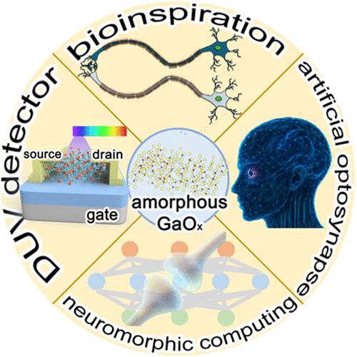
Artificial Solar-Blind Optosynapses Using Amorphous Gallium Oxide Phototransistors for Optical In-Sensor Neuromorphic Applications
Optoelectronic neuromorphic devices, which mimic the functionalities of the human eye and brain neural systems, have attracted significant interest for enabling highly energy-efficient computing systems for next-generation artificial intelligence applications. However, several key challenges persist, including a limited dynamic range for light-induced synaptic weights, low optical photogain, lack of spectral selectivity, and incompatibility with heterogeneous integration. Addressing these issues is essential for unlocking the full potential of optosynaptic devices in advanced AI systems. In this work, we develop artificial solar-blind optoelectronic synaptic devices exhibiting high pattern recognition rates (>92%) in neural network training using ultrawide-bandgap amorphous gallium oxide (a-GaOx) thin-film transistors (TFTs). The device functions through deep ultraviolet (DUV) optically induced potentiation and gate-terminal electrical depression processes, exhibiting excellent plasticity and a wide conductance weight update range. This performance is attributed to its superior TFT switching characteristics, strong DUV photoresponse with a dynamic gain exceeding 108, and UV-triggered persistent photoconductivity (PPC) lasting over 1000 s. Moreover, the device can be fabricated at a low temperature of 450 °C, ensuring compatibility with the complementary metal-oxide–semiconductor (CMOS) back-end-of-line (BEOL) process.
期刊介绍:
ACS Nano, published monthly, serves as an international forum for comprehensive articles on nanoscience and nanotechnology research at the intersections of chemistry, biology, materials science, physics, and engineering. The journal fosters communication among scientists in these communities, facilitating collaboration, new research opportunities, and advancements through discoveries. ACS Nano covers synthesis, assembly, characterization, theory, and simulation of nanostructures, nanobiotechnology, nanofabrication, methods and tools for nanoscience and nanotechnology, and self- and directed-assembly. Alongside original research articles, it offers thorough reviews, perspectives on cutting-edge research, and discussions envisioning the future of nanoscience and nanotechnology.

 求助内容:
求助内容: 应助结果提醒方式:


