Jiale Du, Hao Lu, Bin Hou, Ling Yang, Meng Zhang, Mei Wu, Kaiwen Chen, Tianqi Pan, Yifan Chen, Hailin Liu, Qingyuan Chang, Xiaohua Ma, Yue Hao
{"title":"用于低寄生无金欧姆接触的10.2 W/mm高功率密度x波段GaN-on-Si hemt。","authors":"Jiale Du, Hao Lu, Bin Hou, Ling Yang, Meng Zhang, Mei Wu, Kaiwen Chen, Tianqi Pan, Yifan Chen, Hailin Liu, Qingyuan Chang, Xiaohua Ma, Yue Hao","doi":"10.3390/mi16091067","DOIUrl":null,"url":null,"abstract":"<p><p>To enhance the RF power properties of CMOS-compatible gold-free GaN devices, this work introduces a kind of GaN-on-Si HEMT with a low parasitic regrown ohmic contact technology. Attributed to the highly doped n<sup>+</sup> InGaN regrown layer and smooth morphology of gold-free ohmic stacks, the lowest ohmic contact resistance (<i>R</i><sub>c</sub>) was presented as 0.072 Ω·mm. More importantly, low RF loss and low total dislocation density (TDD) of the Si-based GaN epitaxy were achieved by a designed two-step-graded (TSG) transition structure for the use of scaling-down devices in high-frequency applications. Finally, the fabricated GaN HEMTs on the Si substrate presented a maximum drain current (<i>I</i><sub>drain</sub>) of 1206 mA/mm, a peak transconductance (<i>G</i><sub>m</sub>) of 391 mS/mm, and a breakdown voltage (<i>V</i><sub>BR</sub>) of 169 V. The outstanding material and DC performances strongly encourage a maximum output power density (<i>P</i><sub>out</sub>) of 10.2 W/mm at 8 GHz and drain voltage (<i>V</i><sub>drain</sub>) of 50 V in active pulse mode, which, to our best knowledge, updates the highest power level for gold-free GaN devices on Si substrates. The power results reflect the reliable potential of low parasitic regrown ohmic contact technology for future large-scale CMOS-integrated circuits in RF applications.</p>","PeriodicalId":18508,"journal":{"name":"Micromachines","volume":"16 9","pages":""},"PeriodicalIF":3.0000,"publicationDate":"2025-09-22","publicationTypes":"Journal Article","fieldsOfStudy":null,"isOpenAccess":false,"openAccessPdf":"https://www.ncbi.nlm.nih.gov/pmc/articles/PMC12471317/pdf/","citationCount":"0","resultStr":"{\"title\":\"High Power Density X-Band GaN-on-Si HEMTs with 10.2 W/mm Used by Low Parasitic Gold-Free Ohmic Contact.\",\"authors\":\"Jiale Du, Hao Lu, Bin Hou, Ling Yang, Meng Zhang, Mei Wu, Kaiwen Chen, Tianqi Pan, Yifan Chen, Hailin Liu, Qingyuan Chang, Xiaohua Ma, Yue Hao\",\"doi\":\"10.3390/mi16091067\",\"DOIUrl\":null,\"url\":null,\"abstract\":\"<p><p>To enhance the RF power properties of CMOS-compatible gold-free GaN devices, this work introduces a kind of GaN-on-Si HEMT with a low parasitic regrown ohmic contact technology. Attributed to the highly doped n<sup>+</sup> InGaN regrown layer and smooth morphology of gold-free ohmic stacks, the lowest ohmic contact resistance (<i>R</i><sub>c</sub>) was presented as 0.072 Ω·mm. More importantly, low RF loss and low total dislocation density (TDD) of the Si-based GaN epitaxy were achieved by a designed two-step-graded (TSG) transition structure for the use of scaling-down devices in high-frequency applications. Finally, the fabricated GaN HEMTs on the Si substrate presented a maximum drain current (<i>I</i><sub>drain</sub>) of 1206 mA/mm, a peak transconductance (<i>G</i><sub>m</sub>) of 391 mS/mm, and a breakdown voltage (<i>V</i><sub>BR</sub>) of 169 V. The outstanding material and DC performances strongly encourage a maximum output power density (<i>P</i><sub>out</sub>) of 10.2 W/mm at 8 GHz and drain voltage (<i>V</i><sub>drain</sub>) of 50 V in active pulse mode, which, to our best knowledge, updates the highest power level for gold-free GaN devices on Si substrates. The power results reflect the reliable potential of low parasitic regrown ohmic contact technology for future large-scale CMOS-integrated circuits in RF applications.</p>\",\"PeriodicalId\":18508,\"journal\":{\"name\":\"Micromachines\",\"volume\":\"16 9\",\"pages\":\"\"},\"PeriodicalIF\":3.0000,\"publicationDate\":\"2025-09-22\",\"publicationTypes\":\"Journal Article\",\"fieldsOfStudy\":null,\"isOpenAccess\":false,\"openAccessPdf\":\"https://www.ncbi.nlm.nih.gov/pmc/articles/PMC12471317/pdf/\",\"citationCount\":\"0\",\"resultStr\":null,\"platform\":\"Semanticscholar\",\"paperid\":null,\"PeriodicalName\":\"Micromachines\",\"FirstCategoryId\":\"5\",\"ListUrlMain\":\"https://doi.org/10.3390/mi16091067\",\"RegionNum\":3,\"RegionCategory\":\"工程技术\",\"ArticlePicture\":[],\"TitleCN\":null,\"AbstractTextCN\":null,\"PMCID\":null,\"EPubDate\":\"\",\"PubModel\":\"\",\"JCR\":\"Q2\",\"JCRName\":\"CHEMISTRY, ANALYTICAL\",\"Score\":null,\"Total\":0}","platform":"Semanticscholar","paperid":null,"PeriodicalName":"Micromachines","FirstCategoryId":"5","ListUrlMain":"https://doi.org/10.3390/mi16091067","RegionNum":3,"RegionCategory":"工程技术","ArticlePicture":[],"TitleCN":null,"AbstractTextCN":null,"PMCID":null,"EPubDate":"","PubModel":"","JCR":"Q2","JCRName":"CHEMISTRY, ANALYTICAL","Score":null,"Total":0}
High Power Density X-Band GaN-on-Si HEMTs with 10.2 W/mm Used by Low Parasitic Gold-Free Ohmic Contact.
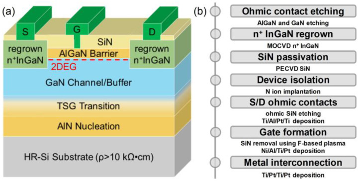
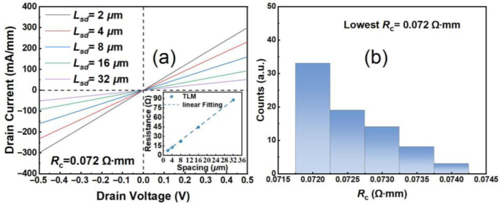
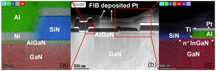
To enhance the RF power properties of CMOS-compatible gold-free GaN devices, this work introduces a kind of GaN-on-Si HEMT with a low parasitic regrown ohmic contact technology. Attributed to the highly doped n+ InGaN regrown layer and smooth morphology of gold-free ohmic stacks, the lowest ohmic contact resistance (Rc) was presented as 0.072 Ω·mm. More importantly, low RF loss and low total dislocation density (TDD) of the Si-based GaN epitaxy were achieved by a designed two-step-graded (TSG) transition structure for the use of scaling-down devices in high-frequency applications. Finally, the fabricated GaN HEMTs on the Si substrate presented a maximum drain current (Idrain) of 1206 mA/mm, a peak transconductance (Gm) of 391 mS/mm, and a breakdown voltage (VBR) of 169 V. The outstanding material and DC performances strongly encourage a maximum output power density (Pout) of 10.2 W/mm at 8 GHz and drain voltage (Vdrain) of 50 V in active pulse mode, which, to our best knowledge, updates the highest power level for gold-free GaN devices on Si substrates. The power results reflect the reliable potential of low parasitic regrown ohmic contact technology for future large-scale CMOS-integrated circuits in RF applications.
期刊介绍:
Micromachines (ISSN 2072-666X) is an international, peer-reviewed open access journal which provides an advanced forum for studies related to micro-scaled machines and micromachinery. It publishes reviews, regular research papers and short communications. Our aim is to encourage scientists to publish their experimental and theoretical results in as much detail as possible. There is no restriction on the length of the papers. The full experimental details must be provided so that the results can be reproduced.
 求助内容:
求助内容: 应助结果提醒方式:


