Bei Ma, Ke Ma, Xinhui Qin, Yingxue Xi, Jin Zhang, Xinyu Yang, Pengfei Yang, Weiguo Liu
{"title":"铪基薄膜厚度对磁控溅射制备掺钇氧化铪铁电器件的微观结构和电性能的影响。","authors":"Bei Ma, Ke Ma, Xinhui Qin, Yingxue Xi, Jin Zhang, Xinyu Yang, Pengfei Yang, Weiguo Liu","doi":"10.3390/mi16091066","DOIUrl":null,"url":null,"abstract":"<p><p>This study employs reactive magnetron sputtering technology to fabricate TiN/Y-HfO<sub>2</sub>/TiN multilayer thin film devices using titanium targets and yttrium-doped high-purity hafnium targets. A systematic investigation was conducted to explore the influence of hafnium-based thin film thickness on the structural and electrical properties of TiN/Y-HfO<sub>2</sub>/TiN thin film devices. Radio frequency magnetron sputtering was utilized to deposit Y-HfO<sub>2</sub> films of varying thicknesses on TiN electrodes by controlling deposition time, with a yttrium doping concentration of 8.24 mol.%. The surface morphology and crystal structure of the thin films were characterized using atomic force microscopy (AFM), Raman spectroscopy, X-ray diffraction (XRD). Results indicate that as film thickness increases, surface roughness and Raman peak intensity increase correspondingly, with the tetragonal phase (t) characteristic peak being most prominent at 65 nm. DC magnetron sputtering was employed to deposit TiN top electrodes, resulting in TiN/Y-HfO<sub>2</sub>/TiN thin film devices. Following rapid thermal annealing at 700 °C, electrical properties were evaluated using a ferroelectric tester. Leakage current density exhibited a decreasing trend with increasing film thickness, while the maximum polarization intensity gradually increased, reaching a maximum of 11.5 μC/cm<sup>2</sup> at 120 nm.</p>","PeriodicalId":18508,"journal":{"name":"Micromachines","volume":"16 9","pages":""},"PeriodicalIF":3.0000,"publicationDate":"2025-09-21","publicationTypes":"Journal Article","fieldsOfStudy":null,"isOpenAccess":false,"openAccessPdf":"https://www.ncbi.nlm.nih.gov/pmc/articles/PMC12471966/pdf/","citationCount":"0","resultStr":"{\"title\":\"Effect of Hafnium-Based Thin Film Thickness on Microstructure and Electrical of Yttrium-Doped Hafnium Oxide Ferroelectric Devices Prepared by Magnetron Sputtering.\",\"authors\":\"Bei Ma, Ke Ma, Xinhui Qin, Yingxue Xi, Jin Zhang, Xinyu Yang, Pengfei Yang, Weiguo Liu\",\"doi\":\"10.3390/mi16091066\",\"DOIUrl\":null,\"url\":null,\"abstract\":\"<p><p>This study employs reactive magnetron sputtering technology to fabricate TiN/Y-HfO<sub>2</sub>/TiN multilayer thin film devices using titanium targets and yttrium-doped high-purity hafnium targets. A systematic investigation was conducted to explore the influence of hafnium-based thin film thickness on the structural and electrical properties of TiN/Y-HfO<sub>2</sub>/TiN thin film devices. Radio frequency magnetron sputtering was utilized to deposit Y-HfO<sub>2</sub> films of varying thicknesses on TiN electrodes by controlling deposition time, with a yttrium doping concentration of 8.24 mol.%. The surface morphology and crystal structure of the thin films were characterized using atomic force microscopy (AFM), Raman spectroscopy, X-ray diffraction (XRD). Results indicate that as film thickness increases, surface roughness and Raman peak intensity increase correspondingly, with the tetragonal phase (t) characteristic peak being most prominent at 65 nm. DC magnetron sputtering was employed to deposit TiN top electrodes, resulting in TiN/Y-HfO<sub>2</sub>/TiN thin film devices. Following rapid thermal annealing at 700 °C, electrical properties were evaluated using a ferroelectric tester. Leakage current density exhibited a decreasing trend with increasing film thickness, while the maximum polarization intensity gradually increased, reaching a maximum of 11.5 μC/cm<sup>2</sup> at 120 nm.</p>\",\"PeriodicalId\":18508,\"journal\":{\"name\":\"Micromachines\",\"volume\":\"16 9\",\"pages\":\"\"},\"PeriodicalIF\":3.0000,\"publicationDate\":\"2025-09-21\",\"publicationTypes\":\"Journal Article\",\"fieldsOfStudy\":null,\"isOpenAccess\":false,\"openAccessPdf\":\"https://www.ncbi.nlm.nih.gov/pmc/articles/PMC12471966/pdf/\",\"citationCount\":\"0\",\"resultStr\":null,\"platform\":\"Semanticscholar\",\"paperid\":null,\"PeriodicalName\":\"Micromachines\",\"FirstCategoryId\":\"5\",\"ListUrlMain\":\"https://doi.org/10.3390/mi16091066\",\"RegionNum\":3,\"RegionCategory\":\"工程技术\",\"ArticlePicture\":[],\"TitleCN\":null,\"AbstractTextCN\":null,\"PMCID\":null,\"EPubDate\":\"\",\"PubModel\":\"\",\"JCR\":\"Q2\",\"JCRName\":\"CHEMISTRY, ANALYTICAL\",\"Score\":null,\"Total\":0}","platform":"Semanticscholar","paperid":null,"PeriodicalName":"Micromachines","FirstCategoryId":"5","ListUrlMain":"https://doi.org/10.3390/mi16091066","RegionNum":3,"RegionCategory":"工程技术","ArticlePicture":[],"TitleCN":null,"AbstractTextCN":null,"PMCID":null,"EPubDate":"","PubModel":"","JCR":"Q2","JCRName":"CHEMISTRY, ANALYTICAL","Score":null,"Total":0}
Effect of Hafnium-Based Thin Film Thickness on Microstructure and Electrical of Yttrium-Doped Hafnium Oxide Ferroelectric Devices Prepared by Magnetron Sputtering.
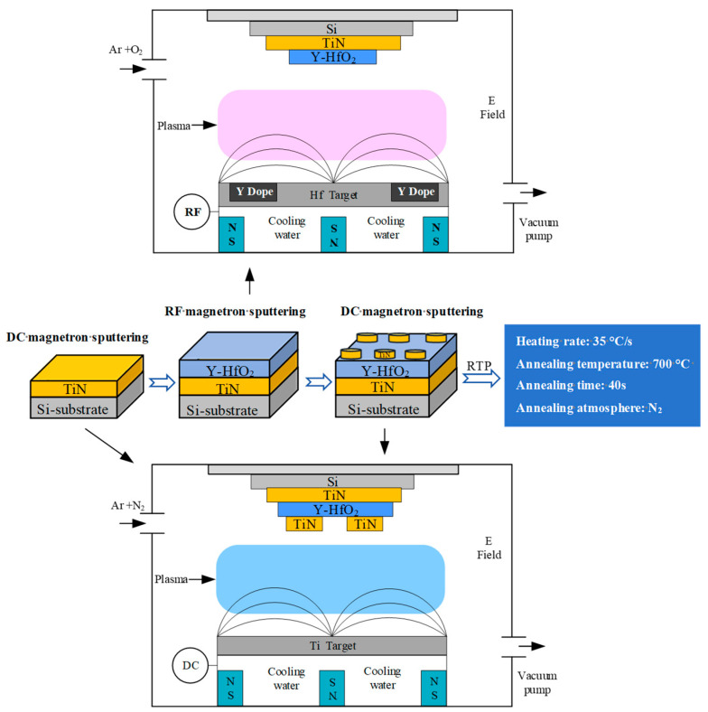
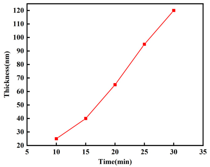
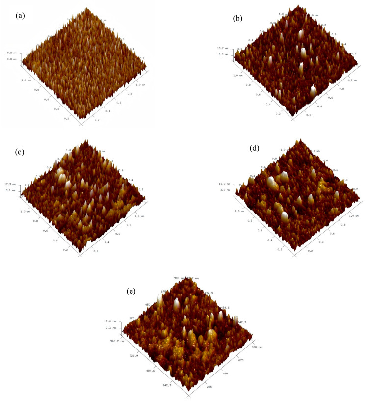
This study employs reactive magnetron sputtering technology to fabricate TiN/Y-HfO2/TiN multilayer thin film devices using titanium targets and yttrium-doped high-purity hafnium targets. A systematic investigation was conducted to explore the influence of hafnium-based thin film thickness on the structural and electrical properties of TiN/Y-HfO2/TiN thin film devices. Radio frequency magnetron sputtering was utilized to deposit Y-HfO2 films of varying thicknesses on TiN electrodes by controlling deposition time, with a yttrium doping concentration of 8.24 mol.%. The surface morphology and crystal structure of the thin films were characterized using atomic force microscopy (AFM), Raman spectroscopy, X-ray diffraction (XRD). Results indicate that as film thickness increases, surface roughness and Raman peak intensity increase correspondingly, with the tetragonal phase (t) characteristic peak being most prominent at 65 nm. DC magnetron sputtering was employed to deposit TiN top electrodes, resulting in TiN/Y-HfO2/TiN thin film devices. Following rapid thermal annealing at 700 °C, electrical properties were evaluated using a ferroelectric tester. Leakage current density exhibited a decreasing trend with increasing film thickness, while the maximum polarization intensity gradually increased, reaching a maximum of 11.5 μC/cm2 at 120 nm.
期刊介绍:
Micromachines (ISSN 2072-666X) is an international, peer-reviewed open access journal which provides an advanced forum for studies related to micro-scaled machines and micromachinery. It publishes reviews, regular research papers and short communications. Our aim is to encourage scientists to publish their experimental and theoretical results in as much detail as possible. There is no restriction on the length of the papers. The full experimental details must be provided so that the results can be reproduced.
 求助内容:
求助内容: 应助结果提醒方式:


