{"title":"通过开关晶体管电流整形提高交叉耦合LC振荡器的相位噪声性能","authors":"Komeil Yazdani, Ali Jalali, Omid Hashemipour","doi":"10.1007/s10470-025-02458-1","DOIUrl":null,"url":null,"abstract":"<div><p>This paper presents an innovative structural modification to enhance the phase noise performance of cross-coupled LC oscillators, a critical component in high-performance RF and wireless communication systems. The proposed architecture reduces phase noise while simultaneously increasing the output oscillation frequency. The key mechanism for noise reduction involves shaping the current of the switch transistors by minimizing their conduction angle precisely at the zero-crossing points of the output oscillation. The oscillator operates in the C-band at 4.02 GHz, making it suitable for radar, satellite communication, and 5G applications. At a 100 kHz offset, the phase noise is measured at − 111.25 dBc/Hz, and at a 1 MHz offset, it reaches − 132.16 dBc/Hz. Simulations were performed using Cadence software with TSMC_0.18 µm_RF CMOS technology at a 1.8 V supply voltage. The oscillator achieves a peak-to-peak output voltage of 2.26 V while consuming only 4.11mW of power. To validate the design under realistic conditions, a full-custom layout was implemented, and post-layout simulations were conducted using extracted parasitics. The post-layout results confirmed minimal degradation in performance and demonstrated that the proposed oscillator maintains competitive figure-of-merit values, highlighting its robustness and practical viability for integrated RF applications.</p></div>","PeriodicalId":7827,"journal":{"name":"Analog Integrated Circuits and Signal Processing","volume":"124 3","pages":""},"PeriodicalIF":1.4000,"publicationDate":"2025-07-23","publicationTypes":"Journal Article","fieldsOfStudy":null,"isOpenAccess":false,"openAccessPdf":"","citationCount":"0","resultStr":"{\"title\":\"Enhancing phase noise performance in cross-coupled LC oscillators through switch transistor current shaping\",\"authors\":\"Komeil Yazdani, Ali Jalali, Omid Hashemipour\",\"doi\":\"10.1007/s10470-025-02458-1\",\"DOIUrl\":null,\"url\":null,\"abstract\":\"<div><p>This paper presents an innovative structural modification to enhance the phase noise performance of cross-coupled LC oscillators, a critical component in high-performance RF and wireless communication systems. The proposed architecture reduces phase noise while simultaneously increasing the output oscillation frequency. The key mechanism for noise reduction involves shaping the current of the switch transistors by minimizing their conduction angle precisely at the zero-crossing points of the output oscillation. The oscillator operates in the C-band at 4.02 GHz, making it suitable for radar, satellite communication, and 5G applications. At a 100 kHz offset, the phase noise is measured at − 111.25 dBc/Hz, and at a 1 MHz offset, it reaches − 132.16 dBc/Hz. Simulations were performed using Cadence software with TSMC_0.18 µm_RF CMOS technology at a 1.8 V supply voltage. The oscillator achieves a peak-to-peak output voltage of 2.26 V while consuming only 4.11mW of power. To validate the design under realistic conditions, a full-custom layout was implemented, and post-layout simulations were conducted using extracted parasitics. The post-layout results confirmed minimal degradation in performance and demonstrated that the proposed oscillator maintains competitive figure-of-merit values, highlighting its robustness and practical viability for integrated RF applications.</p></div>\",\"PeriodicalId\":7827,\"journal\":{\"name\":\"Analog Integrated Circuits and Signal Processing\",\"volume\":\"124 3\",\"pages\":\"\"},\"PeriodicalIF\":1.4000,\"publicationDate\":\"2025-07-23\",\"publicationTypes\":\"Journal Article\",\"fieldsOfStudy\":null,\"isOpenAccess\":false,\"openAccessPdf\":\"\",\"citationCount\":\"0\",\"resultStr\":null,\"platform\":\"Semanticscholar\",\"paperid\":null,\"PeriodicalName\":\"Analog Integrated Circuits and Signal Processing\",\"FirstCategoryId\":\"5\",\"ListUrlMain\":\"https://link.springer.com/article/10.1007/s10470-025-02458-1\",\"RegionNum\":4,\"RegionCategory\":\"工程技术\",\"ArticlePicture\":[],\"TitleCN\":null,\"AbstractTextCN\":null,\"PMCID\":null,\"EPubDate\":\"\",\"PubModel\":\"\",\"JCR\":\"Q4\",\"JCRName\":\"COMPUTER SCIENCE, HARDWARE & ARCHITECTURE\",\"Score\":null,\"Total\":0}","platform":"Semanticscholar","paperid":null,"PeriodicalName":"Analog Integrated Circuits and Signal Processing","FirstCategoryId":"5","ListUrlMain":"https://link.springer.com/article/10.1007/s10470-025-02458-1","RegionNum":4,"RegionCategory":"工程技术","ArticlePicture":[],"TitleCN":null,"AbstractTextCN":null,"PMCID":null,"EPubDate":"","PubModel":"","JCR":"Q4","JCRName":"COMPUTER SCIENCE, HARDWARE & ARCHITECTURE","Score":null,"Total":0}
Enhancing phase noise performance in cross-coupled LC oscillators through switch transistor current shaping
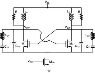
This paper presents an innovative structural modification to enhance the phase noise performance of cross-coupled LC oscillators, a critical component in high-performance RF and wireless communication systems. The proposed architecture reduces phase noise while simultaneously increasing the output oscillation frequency. The key mechanism for noise reduction involves shaping the current of the switch transistors by minimizing their conduction angle precisely at the zero-crossing points of the output oscillation. The oscillator operates in the C-band at 4.02 GHz, making it suitable for radar, satellite communication, and 5G applications. At a 100 kHz offset, the phase noise is measured at − 111.25 dBc/Hz, and at a 1 MHz offset, it reaches − 132.16 dBc/Hz. Simulations were performed using Cadence software with TSMC_0.18 µm_RF CMOS technology at a 1.8 V supply voltage. The oscillator achieves a peak-to-peak output voltage of 2.26 V while consuming only 4.11mW of power. To validate the design under realistic conditions, a full-custom layout was implemented, and post-layout simulations were conducted using extracted parasitics. The post-layout results confirmed minimal degradation in performance and demonstrated that the proposed oscillator maintains competitive figure-of-merit values, highlighting its robustness and practical viability for integrated RF applications.
期刊介绍:
Analog Integrated Circuits and Signal Processing is an archival peer reviewed journal dedicated to the design and application of analog, radio frequency (RF), and mixed signal integrated circuits (ICs) as well as signal processing circuits and systems. It features both new research results and tutorial views and reflects the large volume of cutting-edge research activity in the worldwide field today.
A partial list of topics includes analog and mixed signal interface circuits and systems; analog and RFIC design; data converters; active-RC, switched-capacitor, and continuous-time integrated filters; mixed analog/digital VLSI systems; wireless radio transceivers; clock and data recovery circuits; and high speed optoelectronic circuits and systems.

 求助内容:
求助内容: 应助结果提醒方式:


