{"title":"采用16nm技术的低功耗和面积高效故障模型方法的验证和验证","authors":"Nagapuri Sahithi, Jyothi Lavudya, E. Krishnahari","doi":"10.1007/s10470-025-02424-x","DOIUrl":null,"url":null,"abstract":"<div><p>With the advancement of Very Large-Scale Integration (VLSI), the integration of a high number of transistors on a single chip has significantly improved performance but also increased vulnerability to faults. To address this, we propose and validate fault-tolerant, low-power, and area-efficient circuit designs using 16nm CMOS technology. In this study, a comprehensive fault modeling approach is developed and demonstrated through two representative digital circuits-a full adder and a multiplexer. These circuits are used as case studies to evaluate the proposed fault models under both transient and permanent fault scenarios, including “stuck-at” fault conditions. Two self-repairing multiplexer architectures are introduced: one utilizing additional circuitry to correct faults, and another enabling internal gate-level self-repair. Both designs can detect and recover from single and multiple faults effectively. Furthermore, the full adder architecture incorporates error recovery mechanisms, enhancing system reliability. The proposed designs are simulated and validated using Tanner EDA at 16nm technology node, confirming their efficiency in terms of power, area, and fault tolerance.</p></div>","PeriodicalId":7827,"journal":{"name":"Analog Integrated Circuits and Signal Processing","volume":"124 3","pages":""},"PeriodicalIF":1.4000,"publicationDate":"2025-07-15","publicationTypes":"Journal Article","fieldsOfStudy":null,"isOpenAccess":false,"openAccessPdf":"","citationCount":"0","resultStr":"{\"title\":\"Validation and verification of low power and area efficient fault model methods using 16nm technology\",\"authors\":\"Nagapuri Sahithi, Jyothi Lavudya, E. Krishnahari\",\"doi\":\"10.1007/s10470-025-02424-x\",\"DOIUrl\":null,\"url\":null,\"abstract\":\"<div><p>With the advancement of Very Large-Scale Integration (VLSI), the integration of a high number of transistors on a single chip has significantly improved performance but also increased vulnerability to faults. To address this, we propose and validate fault-tolerant, low-power, and area-efficient circuit designs using 16nm CMOS technology. In this study, a comprehensive fault modeling approach is developed and demonstrated through two representative digital circuits-a full adder and a multiplexer. These circuits are used as case studies to evaluate the proposed fault models under both transient and permanent fault scenarios, including “stuck-at” fault conditions. Two self-repairing multiplexer architectures are introduced: one utilizing additional circuitry to correct faults, and another enabling internal gate-level self-repair. Both designs can detect and recover from single and multiple faults effectively. Furthermore, the full adder architecture incorporates error recovery mechanisms, enhancing system reliability. The proposed designs are simulated and validated using Tanner EDA at 16nm technology node, confirming their efficiency in terms of power, area, and fault tolerance.</p></div>\",\"PeriodicalId\":7827,\"journal\":{\"name\":\"Analog Integrated Circuits and Signal Processing\",\"volume\":\"124 3\",\"pages\":\"\"},\"PeriodicalIF\":1.4000,\"publicationDate\":\"2025-07-15\",\"publicationTypes\":\"Journal Article\",\"fieldsOfStudy\":null,\"isOpenAccess\":false,\"openAccessPdf\":\"\",\"citationCount\":\"0\",\"resultStr\":null,\"platform\":\"Semanticscholar\",\"paperid\":null,\"PeriodicalName\":\"Analog Integrated Circuits and Signal Processing\",\"FirstCategoryId\":\"5\",\"ListUrlMain\":\"https://link.springer.com/article/10.1007/s10470-025-02424-x\",\"RegionNum\":4,\"RegionCategory\":\"工程技术\",\"ArticlePicture\":[],\"TitleCN\":null,\"AbstractTextCN\":null,\"PMCID\":null,\"EPubDate\":\"\",\"PubModel\":\"\",\"JCR\":\"Q4\",\"JCRName\":\"COMPUTER SCIENCE, HARDWARE & ARCHITECTURE\",\"Score\":null,\"Total\":0}","platform":"Semanticscholar","paperid":null,"PeriodicalName":"Analog Integrated Circuits and Signal Processing","FirstCategoryId":"5","ListUrlMain":"https://link.springer.com/article/10.1007/s10470-025-02424-x","RegionNum":4,"RegionCategory":"工程技术","ArticlePicture":[],"TitleCN":null,"AbstractTextCN":null,"PMCID":null,"EPubDate":"","PubModel":"","JCR":"Q4","JCRName":"COMPUTER SCIENCE, HARDWARE & ARCHITECTURE","Score":null,"Total":0}
Validation and verification of low power and area efficient fault model methods using 16nm technology
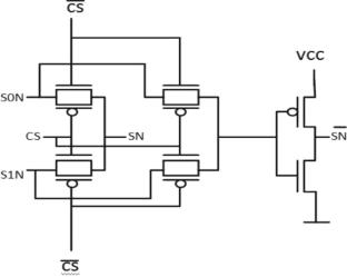
With the advancement of Very Large-Scale Integration (VLSI), the integration of a high number of transistors on a single chip has significantly improved performance but also increased vulnerability to faults. To address this, we propose and validate fault-tolerant, low-power, and area-efficient circuit designs using 16nm CMOS technology. In this study, a comprehensive fault modeling approach is developed and demonstrated through two representative digital circuits-a full adder and a multiplexer. These circuits are used as case studies to evaluate the proposed fault models under both transient and permanent fault scenarios, including “stuck-at” fault conditions. Two self-repairing multiplexer architectures are introduced: one utilizing additional circuitry to correct faults, and another enabling internal gate-level self-repair. Both designs can detect and recover from single and multiple faults effectively. Furthermore, the full adder architecture incorporates error recovery mechanisms, enhancing system reliability. The proposed designs are simulated and validated using Tanner EDA at 16nm technology node, confirming their efficiency in terms of power, area, and fault tolerance.
期刊介绍:
Analog Integrated Circuits and Signal Processing is an archival peer reviewed journal dedicated to the design and application of analog, radio frequency (RF), and mixed signal integrated circuits (ICs) as well as signal processing circuits and systems. It features both new research results and tutorial views and reflects the large volume of cutting-edge research activity in the worldwide field today.
A partial list of topics includes analog and mixed signal interface circuits and systems; analog and RFIC design; data converters; active-RC, switched-capacitor, and continuous-time integrated filters; mixed analog/digital VLSI systems; wireless radio transceivers; clock and data recovery circuits; and high speed optoelectronic circuits and systems.

 求助内容:
求助内容: 应助结果提醒方式:


