N. F. Zikrillaev, Kh. F. Zikrillaev, F. E. Urakova, G. A. Kushiev, E. B. Saitov, D. M. Shukurova, B. Kh. Ibrahimova
{"title":"基于二元化合物GexSi1-x的硅基光伏电池","authors":"N. F. Zikrillaev, Kh. F. Zikrillaev, F. E. Urakova, G. A. Kushiev, E. B. Saitov, D. M. Shukurova, B. Kh. Ibrahimova","doi":"10.3103/S1068375525700127","DOIUrl":null,"url":null,"abstract":"<p>In this paper, the results of the study of photoelectric properties of silicon with binary compounds GexSi1–x are presented. The thermodynamic conditions (<i>Т</i> = 1100–1250°С and <i>t</i> = 5–20 h) and technological modes were determined for low-temperature, two-stage diffusion of impurity atoms of germanium, which made it possible to obtain a material with binary compounds Ge<sub><i>x</i></sub>Si<sub>1–<i>x</i></sub> on the surface and near-surface of silicon with given electrophysical parameters. From the results of the study of the concentration distribution of the formed binary compounds Ge<sub><i>x</i></sub>Si<sub>1–<i>x</i></sub> in silicon, it was established that compounds with the maximum concentration were formed on the surface, and their concentration decreased with depth into the volume of silicon. It was found that the compounds Ge<sub><i>x</i></sub>Si<sub>1–<i>x</i></sub> formed in silicon lead to a change in the forbidden zone width of the original material. It is shown that the change in the forbidden zone width of the original silicon due to the formation of binary compounds Ge<sub><i>x</i></sub>Si<sub>1–<i>x</i></sub> changes one of the fundamental parameters of the material, which, in turn, leads to an expansion of the spectral region of sensitivity, which is typical in the development of efficient photocells with a wide range of solar radiation absorption.</p>","PeriodicalId":782,"journal":{"name":"Surface Engineering and Applied Electrochemistry","volume":"61 2","pages":"234 - 239"},"PeriodicalIF":0.7000,"publicationDate":"2025-06-10","publicationTypes":"Journal Article","fieldsOfStudy":null,"isOpenAccess":false,"openAccessPdf":"","citationCount":"0","resultStr":"{\"title\":\"Photovoltaic Cells Based on Silicon with Binary Compounds GexSi1–x\",\"authors\":\"N. F. Zikrillaev, Kh. F. Zikrillaev, F. E. Urakova, G. A. Kushiev, E. B. Saitov, D. M. Shukurova, B. Kh. Ibrahimova\",\"doi\":\"10.3103/S1068375525700127\",\"DOIUrl\":null,\"url\":null,\"abstract\":\"<p>In this paper, the results of the study of photoelectric properties of silicon with binary compounds GexSi1–x are presented. The thermodynamic conditions (<i>Т</i> = 1100–1250°С and <i>t</i> = 5–20 h) and technological modes were determined for low-temperature, two-stage diffusion of impurity atoms of germanium, which made it possible to obtain a material with binary compounds Ge<sub><i>x</i></sub>Si<sub>1–<i>x</i></sub> on the surface and near-surface of silicon with given electrophysical parameters. From the results of the study of the concentration distribution of the formed binary compounds Ge<sub><i>x</i></sub>Si<sub>1–<i>x</i></sub> in silicon, it was established that compounds with the maximum concentration were formed on the surface, and their concentration decreased with depth into the volume of silicon. It was found that the compounds Ge<sub><i>x</i></sub>Si<sub>1–<i>x</i></sub> formed in silicon lead to a change in the forbidden zone width of the original material. It is shown that the change in the forbidden zone width of the original silicon due to the formation of binary compounds Ge<sub><i>x</i></sub>Si<sub>1–<i>x</i></sub> changes one of the fundamental parameters of the material, which, in turn, leads to an expansion of the spectral region of sensitivity, which is typical in the development of efficient photocells with a wide range of solar radiation absorption.</p>\",\"PeriodicalId\":782,\"journal\":{\"name\":\"Surface Engineering and Applied Electrochemistry\",\"volume\":\"61 2\",\"pages\":\"234 - 239\"},\"PeriodicalIF\":0.7000,\"publicationDate\":\"2025-06-10\",\"publicationTypes\":\"Journal Article\",\"fieldsOfStudy\":null,\"isOpenAccess\":false,\"openAccessPdf\":\"\",\"citationCount\":\"0\",\"resultStr\":null,\"platform\":\"Semanticscholar\",\"paperid\":null,\"PeriodicalName\":\"Surface Engineering and Applied Electrochemistry\",\"FirstCategoryId\":\"1085\",\"ListUrlMain\":\"https://link.springer.com/article/10.3103/S1068375525700127\",\"RegionNum\":0,\"RegionCategory\":null,\"ArticlePicture\":[],\"TitleCN\":null,\"AbstractTextCN\":null,\"PMCID\":null,\"EPubDate\":\"\",\"PubModel\":\"\",\"JCR\":\"Q3\",\"JCRName\":\"Engineering\",\"Score\":null,\"Total\":0}","platform":"Semanticscholar","paperid":null,"PeriodicalName":"Surface Engineering and Applied Electrochemistry","FirstCategoryId":"1085","ListUrlMain":"https://link.springer.com/article/10.3103/S1068375525700127","RegionNum":0,"RegionCategory":null,"ArticlePicture":[],"TitleCN":null,"AbstractTextCN":null,"PMCID":null,"EPubDate":"","PubModel":"","JCR":"Q3","JCRName":"Engineering","Score":null,"Total":0}
Photovoltaic Cells Based on Silicon with Binary Compounds GexSi1–x
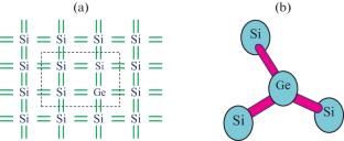
In this paper, the results of the study of photoelectric properties of silicon with binary compounds GexSi1–x are presented. The thermodynamic conditions (Т = 1100–1250°С and t = 5–20 h) and technological modes were determined for low-temperature, two-stage diffusion of impurity atoms of germanium, which made it possible to obtain a material with binary compounds GexSi1–x on the surface and near-surface of silicon with given electrophysical parameters. From the results of the study of the concentration distribution of the formed binary compounds GexSi1–x in silicon, it was established that compounds with the maximum concentration were formed on the surface, and their concentration decreased with depth into the volume of silicon. It was found that the compounds GexSi1–x formed in silicon lead to a change in the forbidden zone width of the original material. It is shown that the change in the forbidden zone width of the original silicon due to the formation of binary compounds GexSi1–x changes one of the fundamental parameters of the material, which, in turn, leads to an expansion of the spectral region of sensitivity, which is typical in the development of efficient photocells with a wide range of solar radiation absorption.
期刊介绍:
Surface Engineering and Applied Electrochemistry is a journal that publishes original and review articles on theory and applications of electroerosion and electrochemical methods for the treatment of materials; physical and chemical methods for the preparation of macro-, micro-, and nanomaterials and their properties; electrical processes in engineering, chemistry, and methods for the processing of biological products and food; and application electromagnetic fields in biological systems.
 求助内容:
求助内容: 应助结果提醒方式:


