{"title":"一种新型的低电压、低功率、高增益全差分CMOS AB类纯电流模电流运算放大器","authors":"Behnam Abdoli, Seyed Javad Azhari","doi":"10.1007/s10470-025-02431-y","DOIUrl":null,"url":null,"abstract":"<div><p>In this paper, a novel fully differential (FD) class AB pure current mode current operational amplifier (COA) is designed and presented. In order to attain highly desired features such as high current gain, very high current drive ratio (I<sub>outmax</sub>/I<sub>bias</sub>) low power consumption, high linearity and good frequency performance, a powerful feedback-based technique is included in the gain stage of the amplifier. Also using the fully differential and class AB structure, implementing FG-MOS transistors in the current output stage along with avoiding high impedance nodes leads to a greatly desired performance in terms of CMRR, PSRR, output current drive capability and low voltage - low power operation which makes the proposed COA suitable for mixed mode and accurate applications. The detailed operation of the proposed COA is far enough discussed, and its small-signal equations are provided. The outstanding properties of the amplifier are verified by Cadence simulations using TSMC 65 nm CMOS technology parameters. To study the robustness of the COA against technology and voltage non-idealities and get results as reliable and practical as measurement, pre-layout and post-layout simulations both plus Monte Carlo analysis are also performed. Under ± 0.9 V supply voltage and 68 µA output bias current, the proposed COA can deliver the output current of ± 1040 mA with THD of − 44 dB, output impedance of 1.88 MΩ, drive ratio (I<sub>outmax</sub>/I<sub>bias</sub>) of 15,300, 108 dB gain, -3dB bandwidth of 14.8 MHz and low consumed power of 282 µw in pre-layout simulation. In post-layout plus Monte–Carlo simulation, the results are as 74 µA, ± 920 mA, − 42 dB, 1.64 MΩ, 12,450, 102 dB, 12.2 MHz and 298 µw for the same arrange of parameters in pre-layout. These results which are as close as possible to the measuring ones prove the remarkable performance of the proposed COA and its superiority over yet artworks.</p></div>","PeriodicalId":7827,"journal":{"name":"Analog Integrated Circuits and Signal Processing","volume":"124 3","pages":""},"PeriodicalIF":1.4000,"publicationDate":"2025-07-08","publicationTypes":"Journal Article","fieldsOfStudy":null,"isOpenAccess":false,"openAccessPdf":"","citationCount":"0","resultStr":"{\"title\":\"A novel low-voltage low-power very high gain fully differential CMOS class AB pure current mode current operational amplifier\",\"authors\":\"Behnam Abdoli, Seyed Javad Azhari\",\"doi\":\"10.1007/s10470-025-02431-y\",\"DOIUrl\":null,\"url\":null,\"abstract\":\"<div><p>In this paper, a novel fully differential (FD) class AB pure current mode current operational amplifier (COA) is designed and presented. In order to attain highly desired features such as high current gain, very high current drive ratio (I<sub>outmax</sub>/I<sub>bias</sub>) low power consumption, high linearity and good frequency performance, a powerful feedback-based technique is included in the gain stage of the amplifier. Also using the fully differential and class AB structure, implementing FG-MOS transistors in the current output stage along with avoiding high impedance nodes leads to a greatly desired performance in terms of CMRR, PSRR, output current drive capability and low voltage - low power operation which makes the proposed COA suitable for mixed mode and accurate applications. The detailed operation of the proposed COA is far enough discussed, and its small-signal equations are provided. The outstanding properties of the amplifier are verified by Cadence simulations using TSMC 65 nm CMOS technology parameters. To study the robustness of the COA against technology and voltage non-idealities and get results as reliable and practical as measurement, pre-layout and post-layout simulations both plus Monte Carlo analysis are also performed. Under ± 0.9 V supply voltage and 68 µA output bias current, the proposed COA can deliver the output current of ± 1040 mA with THD of − 44 dB, output impedance of 1.88 MΩ, drive ratio (I<sub>outmax</sub>/I<sub>bias</sub>) of 15,300, 108 dB gain, -3dB bandwidth of 14.8 MHz and low consumed power of 282 µw in pre-layout simulation. In post-layout plus Monte–Carlo simulation, the results are as 74 µA, ± 920 mA, − 42 dB, 1.64 MΩ, 12,450, 102 dB, 12.2 MHz and 298 µw for the same arrange of parameters in pre-layout. These results which are as close as possible to the measuring ones prove the remarkable performance of the proposed COA and its superiority over yet artworks.</p></div>\",\"PeriodicalId\":7827,\"journal\":{\"name\":\"Analog Integrated Circuits and Signal Processing\",\"volume\":\"124 3\",\"pages\":\"\"},\"PeriodicalIF\":1.4000,\"publicationDate\":\"2025-07-08\",\"publicationTypes\":\"Journal Article\",\"fieldsOfStudy\":null,\"isOpenAccess\":false,\"openAccessPdf\":\"\",\"citationCount\":\"0\",\"resultStr\":null,\"platform\":\"Semanticscholar\",\"paperid\":null,\"PeriodicalName\":\"Analog Integrated Circuits and Signal Processing\",\"FirstCategoryId\":\"5\",\"ListUrlMain\":\"https://link.springer.com/article/10.1007/s10470-025-02431-y\",\"RegionNum\":4,\"RegionCategory\":\"工程技术\",\"ArticlePicture\":[],\"TitleCN\":null,\"AbstractTextCN\":null,\"PMCID\":null,\"EPubDate\":\"\",\"PubModel\":\"\",\"JCR\":\"Q4\",\"JCRName\":\"COMPUTER SCIENCE, HARDWARE & ARCHITECTURE\",\"Score\":null,\"Total\":0}","platform":"Semanticscholar","paperid":null,"PeriodicalName":"Analog Integrated Circuits and Signal Processing","FirstCategoryId":"5","ListUrlMain":"https://link.springer.com/article/10.1007/s10470-025-02431-y","RegionNum":4,"RegionCategory":"工程技术","ArticlePicture":[],"TitleCN":null,"AbstractTextCN":null,"PMCID":null,"EPubDate":"","PubModel":"","JCR":"Q4","JCRName":"COMPUTER SCIENCE, HARDWARE & ARCHITECTURE","Score":null,"Total":0}
A novel low-voltage low-power very high gain fully differential CMOS class AB pure current mode current operational amplifier
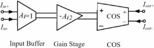
In this paper, a novel fully differential (FD) class AB pure current mode current operational amplifier (COA) is designed and presented. In order to attain highly desired features such as high current gain, very high current drive ratio (Ioutmax/Ibias) low power consumption, high linearity and good frequency performance, a powerful feedback-based technique is included in the gain stage of the amplifier. Also using the fully differential and class AB structure, implementing FG-MOS transistors in the current output stage along with avoiding high impedance nodes leads to a greatly desired performance in terms of CMRR, PSRR, output current drive capability and low voltage - low power operation which makes the proposed COA suitable for mixed mode and accurate applications. The detailed operation of the proposed COA is far enough discussed, and its small-signal equations are provided. The outstanding properties of the amplifier are verified by Cadence simulations using TSMC 65 nm CMOS technology parameters. To study the robustness of the COA against technology and voltage non-idealities and get results as reliable and practical as measurement, pre-layout and post-layout simulations both plus Monte Carlo analysis are also performed. Under ± 0.9 V supply voltage and 68 µA output bias current, the proposed COA can deliver the output current of ± 1040 mA with THD of − 44 dB, output impedance of 1.88 MΩ, drive ratio (Ioutmax/Ibias) of 15,300, 108 dB gain, -3dB bandwidth of 14.8 MHz and low consumed power of 282 µw in pre-layout simulation. In post-layout plus Monte–Carlo simulation, the results are as 74 µA, ± 920 mA, − 42 dB, 1.64 MΩ, 12,450, 102 dB, 12.2 MHz and 298 µw for the same arrange of parameters in pre-layout. These results which are as close as possible to the measuring ones prove the remarkable performance of the proposed COA and its superiority over yet artworks.
期刊介绍:
Analog Integrated Circuits and Signal Processing is an archival peer reviewed journal dedicated to the design and application of analog, radio frequency (RF), and mixed signal integrated circuits (ICs) as well as signal processing circuits and systems. It features both new research results and tutorial views and reflects the large volume of cutting-edge research activity in the worldwide field today.
A partial list of topics includes analog and mixed signal interface circuits and systems; analog and RFIC design; data converters; active-RC, switched-capacitor, and continuous-time integrated filters; mixed analog/digital VLSI systems; wireless radio transceivers; clock and data recovery circuits; and high speed optoelectronic circuits and systems.

 求助内容:
求助内容: 应助结果提醒方式:


