用于易碎纳米结构的两步光电子光刻技术
IF 0.4
4区 工程技术
Q4 ENGINEERING, MULTIDISCIPLINARY
引用次数: 0
摘要
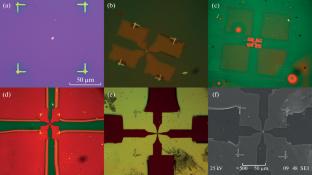
本文提出了一种基于光学显微镜的电子光刻机的补充,用于在电子电阻器上用接触掩模光刻方法在紫外辐射下快速制作大尺寸元件的图像化。该装置加速了固态微纳米结构接触垫的制造,并降低了处理脆弱结构时样品丢失的风险。本文章由计算机程序翻译,如有差异,请以英文原文为准。
Two-Step Photoelectron Lithography for Working with Fragile Nanostructures
An addition to an electron lithograph based on an optical microscope for fast patterning of large-scale elements by the method of contact mask photolithography in ultraviolet radiation on an electronic resistor is presented. The device accelerates the creation of contact pads for solid-state micro- and nanostructures and reduces the risk of sample loss when working with fragile structures.
求助全文
通过发布文献求助,成功后即可免费获取论文全文。
去求助
来源期刊
Instruments and Experimental Techniques
工程技术-工程:综合
CiteScore
1.20
自引率
33.30%
发文量
113
审稿时长
4-8 weeks
期刊介绍:
Instruments and Experimental Techniques is an international peer reviewed journal that publishes reviews describing advanced methods for physical measurements and techniques and original articles that present techniques for physical measurements, principles of operation, design, methods of application, and analysis of the operation of physical instruments used in all fields of experimental physics and when conducting measurements using physical methods and instruments in astronomy, natural sciences, chemistry, biology, medicine, and ecology.
 求助内容:
求助内容: 应助结果提醒方式:


