利用二维金纳米颗粒单层改进纳米肖特基隧道二极管的MIS接口工程

IF 5.7 3区 材料科学 Q2 MATERIALS SCIENCE, MULTIDISCIPLINARY
Tholkappiyan Ramachandran , Hibah Shafeekali , Ashraf Ali , Lianxi Zheng , Haider Butt , Moh'd Rezeq
{"title":"利用二维金纳米颗粒单层改进纳米肖特基隧道二极管的MIS接口工程","authors":"Tholkappiyan Ramachandran ,&nbsp;Hibah Shafeekali ,&nbsp;Ashraf Ali ,&nbsp;Lianxi Zheng ,&nbsp;Haider Butt ,&nbsp;Moh'd Rezeq","doi":"10.1016/j.materresbull.2025.113790","DOIUrl":null,"url":null,"abstract":"<div><div>Schottky diodes are a fundamental component of semiconductor technology, primarily due to their distinctive rectifying behavior at metal–semiconductor (M–S) interfaces. This research investigates the potential of nanoscale Schottky-type contacts to overcome conventional CMOS scaling limitations by leveraging enhanced quantum tunneling and thermionic emission across engineered interfaces. A novel metal–insulator–semiconductor (MIS) diode architecture is developed by integrating a two-dimensional (2D) monolayer of gold nanoparticles (Au-NPs) onto an n-type silicon (n-Si) substrate, separated by a thin SiO₂ insulating layer. The study systematically explores the influence of Au-NP diameters (20 nm, 30 nm, and 40 nm) on charge transport mechanisms. Nanoparticle monolayers were fabricated via drop-casting under an external electric field to ensure uniform alignment. Structural characterization confirmed well-distributed and high-quality monolayers. Electrical measurements revealed a strong size-dependent behavior: the 20 nm Au-NP-based diode exhibited the highest reverse-bias tunneling current (–0.2234 mA at –3.6 V), the lowest contact resistance, and the smallest effective contact area due to enhanced electric field localization. Diodes with larger particles showed reduced tunneling efficiency and higher resistive losses. COMSOL simulations supported the experimental findings, demonstrating that smaller Au-NPs generate higher electric field intensities (4.15 × 10⁸ V/m) at the interface, significantly boosting tunneling probability. These results demonstrate that Au-NP monolayers can be precisely engineered to enhance charge transport across MIS junctions, offering a scalable pathway for high-performance nanoelectronic and optoelectronic devices.</div></div>","PeriodicalId":18265,"journal":{"name":"Materials Research Bulletin","volume":"194 ","pages":"Article 113790"},"PeriodicalIF":5.7000,"publicationDate":"2025-09-17","publicationTypes":"Journal Article","fieldsOfStudy":null,"isOpenAccess":false,"openAccessPdf":"","citationCount":"0","resultStr":"{\"title\":\"Engineering of MIS interfaces using 2D gold nanoparticle monolayers for improved nano-Schottky tunneling diodes\",\"authors\":\"Tholkappiyan Ramachandran ,&nbsp;Hibah Shafeekali ,&nbsp;Ashraf Ali ,&nbsp;Lianxi Zheng ,&nbsp;Haider Butt ,&nbsp;Moh'd Rezeq\",\"doi\":\"10.1016/j.materresbull.2025.113790\",\"DOIUrl\":null,\"url\":null,\"abstract\":\"<div><div>Schottky diodes are a fundamental component of semiconductor technology, primarily due to their distinctive rectifying behavior at metal–semiconductor (M–S) interfaces. This research investigates the potential of nanoscale Schottky-type contacts to overcome conventional CMOS scaling limitations by leveraging enhanced quantum tunneling and thermionic emission across engineered interfaces. A novel metal–insulator–semiconductor (MIS) diode architecture is developed by integrating a two-dimensional (2D) monolayer of gold nanoparticles (Au-NPs) onto an n-type silicon (n-Si) substrate, separated by a thin SiO₂ insulating layer. The study systematically explores the influence of Au-NP diameters (20 nm, 30 nm, and 40 nm) on charge transport mechanisms. Nanoparticle monolayers were fabricated via drop-casting under an external electric field to ensure uniform alignment. Structural characterization confirmed well-distributed and high-quality monolayers. Electrical measurements revealed a strong size-dependent behavior: the 20 nm Au-NP-based diode exhibited the highest reverse-bias tunneling current (–0.2234 mA at –3.6 V), the lowest contact resistance, and the smallest effective contact area due to enhanced electric field localization. Diodes with larger particles showed reduced tunneling efficiency and higher resistive losses. COMSOL simulations supported the experimental findings, demonstrating that smaller Au-NPs generate higher electric field intensities (4.15 × 10⁸ V/m) at the interface, significantly boosting tunneling probability. These results demonstrate that Au-NP monolayers can be precisely engineered to enhance charge transport across MIS junctions, offering a scalable pathway for high-performance nanoelectronic and optoelectronic devices.</div></div>\",\"PeriodicalId\":18265,\"journal\":{\"name\":\"Materials Research Bulletin\",\"volume\":\"194 \",\"pages\":\"Article 113790\"},\"PeriodicalIF\":5.7000,\"publicationDate\":\"2025-09-17\",\"publicationTypes\":\"Journal Article\",\"fieldsOfStudy\":null,\"isOpenAccess\":false,\"openAccessPdf\":\"\",\"citationCount\":\"0\",\"resultStr\":null,\"platform\":\"Semanticscholar\",\"paperid\":null,\"PeriodicalName\":\"Materials Research Bulletin\",\"FirstCategoryId\":\"88\",\"ListUrlMain\":\"https://www.sciencedirect.com/science/article/pii/S0025540825004970\",\"RegionNum\":3,\"RegionCategory\":\"材料科学\",\"ArticlePicture\":[],\"TitleCN\":null,\"AbstractTextCN\":null,\"PMCID\":null,\"EPubDate\":\"\",\"PubModel\":\"\",\"JCR\":\"Q2\",\"JCRName\":\"MATERIALS SCIENCE, MULTIDISCIPLINARY\",\"Score\":null,\"Total\":0}","platform":"Semanticscholar","paperid":null,"PeriodicalName":"Materials Research Bulletin","FirstCategoryId":"88","ListUrlMain":"https://www.sciencedirect.com/science/article/pii/S0025540825004970","RegionNum":3,"RegionCategory":"材料科学","ArticlePicture":[],"TitleCN":null,"AbstractTextCN":null,"PMCID":null,"EPubDate":"","PubModel":"","JCR":"Q2","JCRName":"MATERIALS SCIENCE, MULTIDISCIPLINARY","Score":null,"Total":0}
引用次数: 0

摘要

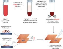
肖特基二极管是半导体技术的基本组成部分,主要是由于它们在金属半导体(M-S)界面上的独特整流行为。本研究探讨了纳米肖特基型触点的潜力,通过利用增强的量子隧道和热离子发射跨越工程界面,克服传统CMOS的缩放限制。一种新型的金属绝缘体半导体(MIS)二极管结构是通过将二维(2D)单层金纳米颗粒(Au-NPs)集成到n型硅(n-Si)衬底上,并由薄的sio2绝缘层隔开。该研究系统地探讨了Au-NP直径(20 nm、30 nm和40 nm)对电荷输运机制的影响。在外加电场作用下,采用滴铸法制备了纳米颗粒单层膜,以保证其排列均匀。结构表征证实了均匀分布和高质量的单层膜。电学测量结果显示,基于au - np的20 nm二极管具有很强的尺寸依赖性:由于增强的电场定位,该二极管具有最高的反向偏置隧道电流(-0.2234 mA, -3.6 V),最低的接触电阻和最小的有效接触面积。颗粒较大的二极管隧道效率降低,电阻损耗增大。COMSOL模拟支持实验结果,表明较小的Au-NPs在界面处产生更高的电场强度(4.15 × 10⁸V/m),显著提高了隧穿概率。这些结果表明,Au-NP单层可以精确地设计来增强MIS结之间的电荷传输,为高性能纳米电子和光电子器件提供了可扩展的途径。
本文章由计算机程序翻译,如有差异,请以英文原文为准。

Engineering of MIS interfaces using 2D gold nanoparticle monolayers for improved nano-Schottky tunneling diodes

Engineering of MIS interfaces using 2D gold nanoparticle monolayers for improved nano-Schottky tunneling diodes
Schottky diodes are a fundamental component of semiconductor technology, primarily due to their distinctive rectifying behavior at metal–semiconductor (M–S) interfaces. This research investigates the potential of nanoscale Schottky-type contacts to overcome conventional CMOS scaling limitations by leveraging enhanced quantum tunneling and thermionic emission across engineered interfaces. A novel metal–insulator–semiconductor (MIS) diode architecture is developed by integrating a two-dimensional (2D) monolayer of gold nanoparticles (Au-NPs) onto an n-type silicon (n-Si) substrate, separated by a thin SiO₂ insulating layer. The study systematically explores the influence of Au-NP diameters (20 nm, 30 nm, and 40 nm) on charge transport mechanisms. Nanoparticle monolayers were fabricated via drop-casting under an external electric field to ensure uniform alignment. Structural characterization confirmed well-distributed and high-quality monolayers. Electrical measurements revealed a strong size-dependent behavior: the 20 nm Au-NP-based diode exhibited the highest reverse-bias tunneling current (–0.2234 mA at –3.6 V), the lowest contact resistance, and the smallest effective contact area due to enhanced electric field localization. Diodes with larger particles showed reduced tunneling efficiency and higher resistive losses. COMSOL simulations supported the experimental findings, demonstrating that smaller Au-NPs generate higher electric field intensities (4.15 × 10⁸ V/m) at the interface, significantly boosting tunneling probability. These results demonstrate that Au-NP monolayers can be precisely engineered to enhance charge transport across MIS junctions, offering a scalable pathway for high-performance nanoelectronic and optoelectronic devices.
求助全文
通过发布文献求助,成功后即可免费获取论文全文。 去求助
来源期刊
Materials Research Bulletin
Materials Research Bulletin 工程技术-材料科学:综合
CiteScore
9.80
自引率
5.60%
发文量
372
审稿时长
42 days
期刊介绍: Materials Research Bulletin is an international journal reporting high-impact research on processing-structure-property relationships in functional materials and nanomaterials with interesting electronic, magnetic, optical, thermal, mechanical or catalytic properties. Papers purely on thermodynamics or theoretical calculations (e.g., density functional theory) do not fall within the scope of the journal unless they also demonstrate a clear link to physical properties. Topics covered include functional materials (e.g., dielectrics, pyroelectrics, piezoelectrics, ferroelectrics, relaxors, thermoelectrics, etc.); electrochemistry and solid-state ionics (e.g., photovoltaics, batteries, sensors, and fuel cells); nanomaterials, graphene, and nanocomposites; luminescence and photocatalysis; crystal-structure and defect-structure analysis; novel electronics; non-crystalline solids; flexible electronics; protein-material interactions; and polymeric ion-exchange membranes.
×
引用
GB/T 7714-2015
复制
MLA
复制
APA
复制
导出至
BibTeX EndNote RefMan NoteFirst NoteExpress
×
提示
您的信息不完整,为了账户安全,请先补充。
现在去补充
×
提示
您因"违规操作"
具体请查看互助需知
我知道了
×
提示
确定
请完成安全验证×
copy
已复制链接
快去分享给好友吧!
我知道了
右上角分享
点击右上角分享
0
联系我们:info@booksci.cn Book学术提供免费学术资源搜索服务,方便国内外学者检索中英文文献。致力于提供最便捷和优质的服务体验。 Copyright © 2023 布克学术 All rights reserved.
京ICP备2023020795号-1
ghs 京公网安备 11010802042870号
Book学术文献互助
Book学术文献互助群
群 号:604180095
Book学术官方微信