原位聚合聚吡咯导电膜作为导电种子层用于印刷电路板的孔金属化及盲孔电镀填充行为

IF 4.5 2区 化学 Q2 POLYMER SCIENCE
Xiao Zhang , Xixun Shen , Runlin Wang , Zihao Zhang , Wei Huang , Qunjie Xu , Zhenni Kang , Junfeng He
{"title":"原位聚合聚吡咯导电膜作为导电种子层用于印刷电路板的孔金属化及盲孔电镀填充行为","authors":"Xiao Zhang ,&nbsp;Xixun Shen ,&nbsp;Runlin Wang ,&nbsp;Zihao Zhang ,&nbsp;Wei Huang ,&nbsp;Qunjie Xu ,&nbsp;Zhenni Kang ,&nbsp;Junfeng He","doi":"10.1016/j.polymer.2025.129140","DOIUrl":null,"url":null,"abstract":"<div><div>At present, the hole metallization of printed Circuit Boards (PCBs) is achieved through using traditional electroless copper as a conductive seed, accompanied by an electroplating copper filling process. This method has serious environmental issues due to the carcinogenic formaldehyde and recalcitrant chelating agents in the electroless plating solution. To address this issue, a green polymer polypyrrole conductive film is proposed to replace traditional electroless copper as a conductive seed layer for the metallization of PCB. The polypyrrole film is formed via in-situ polymerization of pyrrole monomers on blind-hole walls. The cross-sectional SEM and EDS analysis confirmed that the polypyrrole film was uniformly formed on the walls of blind holes. The polypyrrole conductive layer exhibits a low sheet resistance of 1.45 kΩ/sq. Electrochemical characterizations demonstrate rapid copper electrodeposition on this conductive polymer layer. The contact angle measurements also demonstrate that the polypyrrole conductive film enhances substrate wettability, facilitating electrolyte infiltration into the vias. The filling experiment shows that dense super filling of copper in blind holes can be achieved within about 70 min. Thermal shock experiments confirm excellent adhesion of the plated copper. These results demonstrate that the polypyrrole conductive film represents a highly promising material to replace traditional electroless copper as the conductive seed layer for the metallization of PCB.</div></div>","PeriodicalId":405,"journal":{"name":"Polymer","volume":"339 ","pages":"Article 129140"},"PeriodicalIF":4.5000,"publicationDate":"2025-09-25","publicationTypes":"Journal Article","fieldsOfStudy":null,"isOpenAccess":false,"openAccessPdf":"","citationCount":"0","resultStr":"{\"title\":\"Polypyrrole conductive film formed by in-situ polymerization as a conductive seed layer for hole metallization of printed circuit boards and blind hole electroplating filling behavior\",\"authors\":\"Xiao Zhang ,&nbsp;Xixun Shen ,&nbsp;Runlin Wang ,&nbsp;Zihao Zhang ,&nbsp;Wei Huang ,&nbsp;Qunjie Xu ,&nbsp;Zhenni Kang ,&nbsp;Junfeng He\",\"doi\":\"10.1016/j.polymer.2025.129140\",\"DOIUrl\":null,\"url\":null,\"abstract\":\"<div><div>At present, the hole metallization of printed Circuit Boards (PCBs) is achieved through using traditional electroless copper as a conductive seed, accompanied by an electroplating copper filling process. This method has serious environmental issues due to the carcinogenic formaldehyde and recalcitrant chelating agents in the electroless plating solution. To address this issue, a green polymer polypyrrole conductive film is proposed to replace traditional electroless copper as a conductive seed layer for the metallization of PCB. The polypyrrole film is formed via in-situ polymerization of pyrrole monomers on blind-hole walls. The cross-sectional SEM and EDS analysis confirmed that the polypyrrole film was uniformly formed on the walls of blind holes. The polypyrrole conductive layer exhibits a low sheet resistance of 1.45 kΩ/sq. Electrochemical characterizations demonstrate rapid copper electrodeposition on this conductive polymer layer. The contact angle measurements also demonstrate that the polypyrrole conductive film enhances substrate wettability, facilitating electrolyte infiltration into the vias. The filling experiment shows that dense super filling of copper in blind holes can be achieved within about 70 min. Thermal shock experiments confirm excellent adhesion of the plated copper. These results demonstrate that the polypyrrole conductive film represents a highly promising material to replace traditional electroless copper as the conductive seed layer for the metallization of PCB.</div></div>\",\"PeriodicalId\":405,\"journal\":{\"name\":\"Polymer\",\"volume\":\"339 \",\"pages\":\"Article 129140\"},\"PeriodicalIF\":4.5000,\"publicationDate\":\"2025-09-25\",\"publicationTypes\":\"Journal Article\",\"fieldsOfStudy\":null,\"isOpenAccess\":false,\"openAccessPdf\":\"\",\"citationCount\":\"0\",\"resultStr\":null,\"platform\":\"Semanticscholar\",\"paperid\":null,\"PeriodicalName\":\"Polymer\",\"FirstCategoryId\":\"92\",\"ListUrlMain\":\"https://www.sciencedirect.com/science/article/pii/S0032386125011267\",\"RegionNum\":2,\"RegionCategory\":\"化学\",\"ArticlePicture\":[],\"TitleCN\":null,\"AbstractTextCN\":null,\"PMCID\":null,\"EPubDate\":\"\",\"PubModel\":\"\",\"JCR\":\"Q2\",\"JCRName\":\"POLYMER SCIENCE\",\"Score\":null,\"Total\":0}","platform":"Semanticscholar","paperid":null,"PeriodicalName":"Polymer","FirstCategoryId":"92","ListUrlMain":"https://www.sciencedirect.com/science/article/pii/S0032386125011267","RegionNum":2,"RegionCategory":"化学","ArticlePicture":[],"TitleCN":null,"AbstractTextCN":null,"PMCID":null,"EPubDate":"","PubModel":"","JCR":"Q2","JCRName":"POLYMER SCIENCE","Score":null,"Total":0}
引用次数: 0

摘要

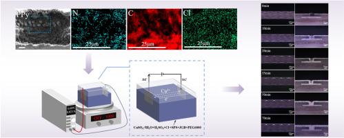
目前,印刷电路板(pcb)的孔金属化是通过使用传统的化学铜作为导电种子,并辅以电镀铜填充工艺来实现的。由于化学镀液中含有致癌物甲醛和顽固的螯合剂,这种方法存在严重的环境问题。为了解决这一问题,提出了一种绿色聚合物聚吡咯导电膜来取代传统的化学铜作为PCB金属化的导电种子层。聚吡咯薄膜是通过在盲孔壁上原位聚合吡咯单体形成的。透射电镜和能谱分析证实,聚吡咯薄膜在盲孔壁上均匀形成。聚吡咯导电层的片电阻较低,为1.45 kΩ/sq。电化学表征表明铜在导电聚合物层上快速电沉积。接触角测量还表明,聚吡咯导电膜增强了衬底的润湿性,促进了电解质渗入过孔。充填试验表明,在70分钟左右的时间内,可实现盲孔内铜的致密超充填。热冲击实验证实了镀铜的良好附着力。这些结果表明,聚吡咯导电膜是一种非常有前途的材料,可以取代传统的化学铜作为PCB金属化的导电种子层。
本文章由计算机程序翻译,如有差异,请以英文原文为准。

Polypyrrole conductive film formed by in-situ polymerization as a conductive seed layer for hole metallization of printed circuit boards and blind hole electroplating filling behavior

Polypyrrole conductive film formed by in-situ polymerization as a conductive seed layer for hole metallization of printed circuit boards and blind hole electroplating filling behavior

Polypyrrole conductive film formed by in-situ polymerization as a conductive seed layer for hole metallization of printed circuit boards and blind hole electroplating filling behavior
At present, the hole metallization of printed Circuit Boards (PCBs) is achieved through using traditional electroless copper as a conductive seed, accompanied by an electroplating copper filling process. This method has serious environmental issues due to the carcinogenic formaldehyde and recalcitrant chelating agents in the electroless plating solution. To address this issue, a green polymer polypyrrole conductive film is proposed to replace traditional electroless copper as a conductive seed layer for the metallization of PCB. The polypyrrole film is formed via in-situ polymerization of pyrrole monomers on blind-hole walls. The cross-sectional SEM and EDS analysis confirmed that the polypyrrole film was uniformly formed on the walls of blind holes. The polypyrrole conductive layer exhibits a low sheet resistance of 1.45 kΩ/sq. Electrochemical characterizations demonstrate rapid copper electrodeposition on this conductive polymer layer. The contact angle measurements also demonstrate that the polypyrrole conductive film enhances substrate wettability, facilitating electrolyte infiltration into the vias. The filling experiment shows that dense super filling of copper in blind holes can be achieved within about 70 min. Thermal shock experiments confirm excellent adhesion of the plated copper. These results demonstrate that the polypyrrole conductive film represents a highly promising material to replace traditional electroless copper as the conductive seed layer for the metallization of PCB.
求助全文
通过发布文献求助,成功后即可免费获取论文全文。 去求助
来源期刊
Polymer
Polymer 化学-高分子科学
CiteScore
7.90
自引率
8.70%
发文量
959
审稿时长
32 days
期刊介绍: Polymer is an interdisciplinary journal dedicated to publishing innovative and significant advances in Polymer Physics, Chemistry and Technology. We welcome submissions on polymer hybrids, nanocomposites, characterisation and self-assembly. Polymer also publishes work on the technological application of polymers in energy and optoelectronics. The main scope is covered but not limited to the following core areas: Polymer Materials Nanocomposites and hybrid nanomaterials Polymer blends, films, fibres, networks and porous materials Physical Characterization Characterisation, modelling and simulation* of molecular and materials properties in bulk, solution, and thin films Polymer Engineering Advanced multiscale processing methods Polymer Synthesis, Modification and Self-assembly Including designer polymer architectures, mechanisms and kinetics, and supramolecular polymerization Technological Applications Polymers for energy generation and storage Polymer membranes for separation technology Polymers for opto- and microelectronics.
×
引用
GB/T 7714-2015
复制
MLA
复制
APA
复制
导出至
BibTeX EndNote RefMan NoteFirst NoteExpress
×
提示
您的信息不完整,为了账户安全,请先补充。
现在去补充
×
提示
您因"违规操作"
具体请查看互助需知
我知道了
×
提示
确定
请完成安全验证×
copy
已复制链接
快去分享给好友吧!
我知道了
右上角分享
点击右上角分享
0
联系我们:info@booksci.cn Book学术提供免费学术资源搜索服务,方便国内外学者检索中英文文献。致力于提供最便捷和优质的服务体验。 Copyright © 2023 布克学术 All rights reserved.
京ICP备2023020795号-1
ghs 京公网安备 11010802042870号
Book学术文献互助
Book学术文献互助群
群 号:604180095
Book学术官方微信