二维六方氮化硼表面热蒸发生长卤化锡钙钛矿薄膜
IF 18.2
1区 材料科学
Q1 CHEMISTRY, PHYSICAL
引用次数: 0
摘要
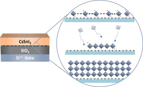
卤化锡钙钛矿具有低的空穴有效质量和适宜的空穴密度,可作为p型晶体管的沟道材料。然而,薄膜结晶不受控制,导致过量的锡空位和自p掺杂。在这项研究中,我们报告了一种在无悬键六方氮化硼(hBN)表面热蒸发生长三维(3D)卤化锡钙钛矿薄膜的简便方法。hBN作为栅极介电/通道中间层转移到SiO2上,提供疏水表面,通过降低成核位密度、增大核尺寸和促进均匀取向的扩大晶粒的形成来促进CsSnI3薄膜的结晶。在hBN上生长的CsSnI3薄膜针孔和晶界减少,锡空位浓度降低。使用这些薄膜的薄膜晶体管在没有任何添加剂的情况下具有大电流调制的加速电荷输运。所提出的策略可以促进集成钙钛矿电子器件中无缺陷钙钛矿通道层的工程设计。本文章由计算机程序翻译,如有差异,请以英文原文为准。
Growth of Tin Halide Perovskite Film on Two-Dimensional Hexagonal Boron Nitride via Thermal Evaporation
Tin halide perovskites have served as channel materials for p-type transistors owing to their low hole effective mass and suitable hole density. However, they suffer from uncontrolled film crystallization, leading to excessive tin vacancies and self-p-doping. In this study, we report a facile way to grow three-dimensional (3D) tin halide perovskite films by thermal evaporation on a dangling-bond-free hexagonal boron nitride (hBN) surface. The hBN, transferred onto SiO2 as a gate dielectric/channel interlayer, offers a hydrophobic surface that promotes the crystallization of CsSnI3 films by reducing the nucleation site density, increasing the nuclei size, and promoting the formation of uniformly oriented enlarged grains. CsSnI3 films grown on hBN exhibit reduced pinholes and grain boundaries, reducing the concentration of tin vacancies. Thin-film transistors using these films demonstrate accelerated charge transport with large current modulation without any additives. The proposed strategy can facilitate the engineering of defect-free perovskite channel layers for integrated perovskite electronics.
求助全文
通过发布文献求助,成功后即可免费获取论文全文。
去求助
来源期刊
ACS Energy Letters
Energy-Renewable Energy, Sustainability and the Environment
CiteScore
31.20
自引率
5.00%
发文量
469
审稿时长
1 months
期刊介绍:
ACS Energy Letters is a monthly journal that publishes papers reporting new scientific advances in energy research. The journal focuses on topics that are of interest to scientists working in the fundamental and applied sciences. Rapid publication is a central criterion for acceptance, and the journal is known for its quick publication times, with an average of 4-6 weeks from submission to web publication in As Soon As Publishable format.
ACS Energy Letters is ranked as the number one journal in the Web of Science Electrochemistry category. It also ranks within the top 10 journals for Physical Chemistry, Energy & Fuels, and Nanoscience & Nanotechnology.
The journal offers several types of articles, including Letters, Energy Express, Perspectives, Reviews, Editorials, Viewpoints and Energy Focus. Additionally, authors have the option to submit videos that summarize or support the information presented in a Perspective or Review article, which can be highlighted on the journal's website. ACS Energy Letters is abstracted and indexed in Chemical Abstracts Service/SciFinder, EBSCO-summon, PubMed, Web of Science, Scopus and Portico.
 求助内容:
求助内容: 应助结果提醒方式:


