研究基于ptse2的电子器件中的欧姆接触
IF 6.2
3区 材料科学
Q2 CHEMISTRY, PHYSICAL
引用次数: 0
摘要
过渡金属二硫族化合物(TMDs)由于其独特的电学和结构特性,在下一代电子器件中具有重要的应用前景。然而,基于tmd的器件的性能受到金属-半导体触点性质的强烈影响。实现低电阻、稳定和高效的接触仍然是充分发挥TMD材料在实际应用中的潜力的关键挑战和关键因素。特别是二硒化铂(PtSe2)由于其可调谐的电子特性和可扩展合成的适用性而成为令人信服的候选者。先进的制造和精确的接触工程是最小化接口退化和最大化器件性能的关键。在本研究中,在c平面蓝宝石上合成了外延PtSe2层,为可扩展器件的制造提供了理想的平台。采用双阻发射技术结合单区硫化方法制备了ptse2基电子结构。通过对镍(Ni)和铂(Pt)作为源极/漏极的评价,重点进行了系统的接触工程研究。电学表征表明,与Ni相比,Pt的接触电阻降低了三倍。相关扫描透射电子显微镜(STEM)和能量色散x射线光谱(EDX)证实,Pt向衬底扩散而不破坏PtSe2层,而Ni则导致严重的顶层降解。为了研究厚度对器件性能的影响,我们在具有Pt/Au触点的TLM (Transfer Length Method)结构中逐渐减小了PtSe2的厚度。薄膜在1.5 nm以下保持了连续的形态和稳定的电学行为,而进一步减小导致表面粗糙度增加,空洞形成,片电阻和接触电阻显着上升。这些发现强调了接触工程和界面质量在保持薄膜完整性和优化器件性能方面的关键作用。此外,该结果为将PtSe2和相关TMDs集成到高性能电子应用中提供了可扩展的制造途径。本文章由计算机程序翻译,如有差异,请以英文原文为准。
Investigating Ohmic contacts in PtSe2-based electronics
Transition metal dichalcogenides (TMDs) hold significant promise for next-generation electronic devices due to their unique electrical and structural properties. However, the performance of TMD-based devices is strongly influenced by the nature of the metal–semiconductor contacts. Achieving low-resistance, stable, and efficient contacts remains a key challenge and a crucial factor in fully realizing the potential of TMD materials in practical applications. In particular, platinum diselenide (PtSe2) has emerged as a compelling candidate due to its tunable electronic properties and suitability for scalable synthesis. Advanced fabrication and precise contact engineering are key to minimizing interfacial degradation and maximizing device performance.
In this study, epitaxial PtSe2 layers were synthesized on c-plane sapphire, providing an ideal platform for scalable device fabrication. PtSe2-based electronic structures were fabricated by a two-resist lift-off technique combined with a one-zone chalcogenization approach.
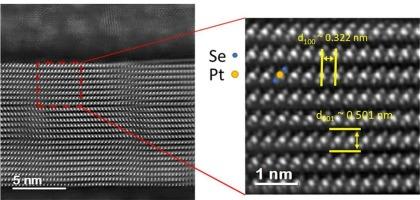
We have focused on the systematical contact engineering investigation by evaluating nickel (Ni) and platinum (Pt) as source/drain electrodes. Electrical characterization showed a threefold reduction in Pt contact resistance as compared to Ni. Correlative scanning transmission electron microscopy (STEM) and energy-dispersive X-ray spectroscopy (EDX) confirm that Pt diffuses toward the substrate without disrupting the PtSe2 layers, whereas Ni induces severe top-layer degradation.
To investigate the impact of thickness on device performance, we gradually reduced the thickness of few-layer PtSe2 in Transfer Length Method (TLM) structures with Pt/Au contacts. The films maintained continuous morphology and stable electrical behavior down to 1.5 nm, while further reduction led to increased surface roughness, void formation, and a notable rise in sheet and contact resistance.
These findings highlight the critical role of contact engineering and interface quality in preserving film integrity and optimizing device performance. Moreover, the results offer a scalable fabrication pathway for integrating PtSe2 and related TMDs into high-performance electronic applications.
求助全文
通过发布文献求助,成功后即可免费获取论文全文。
去求助
来源期刊
FlatChem
Multiple-
CiteScore
8.40
自引率
6.50%
发文量
104
审稿时长
26 days
期刊介绍:
FlatChem - Chemistry of Flat Materials, a new voice in the community, publishes original and significant, cutting-edge research related to the chemistry of graphene and related 2D & layered materials. The overall aim of the journal is to combine the chemistry and applications of these materials, where the submission of communications, full papers, and concepts should contain chemistry in a materials context, which can be both experimental and/or theoretical. In addition to original research articles, FlatChem also offers reviews, minireviews, highlights and perspectives on the future of this research area with the scientific leaders in fields related to Flat Materials. Topics of interest include, but are not limited to, the following: -Design, synthesis, applications and investigation of graphene, graphene related materials and other 2D & layered materials (for example Silicene, Germanene, Phosphorene, MXenes, Boron nitride, Transition metal dichalcogenides) -Characterization of these materials using all forms of spectroscopy and microscopy techniques -Chemical modification or functionalization and dispersion of these materials, as well as interactions with other materials -Exploring the surface chemistry of these materials for applications in: Sensors or detectors in electrochemical/Lab on a Chip devices, Composite materials, Membranes, Environment technology, Catalysis for energy storage and conversion (for example fuel cells, supercapacitors, batteries, hydrogen storage), Biomedical technology (drug delivery, biosensing, bioimaging)
 求助内容:
求助内容: 应助结果提醒方式:


