{"title":"利用氧空位变化识别氧化铟镓锌薄膜的化学结构","authors":"Jong-Cheol Lee, , , Jinheon Choi, , , Tackhwi Lee, , , Minsik Kim, , , Seongmin Ahn, , , Junghan Lee, , , Sungho Lee, , , Jihyun Kho, , , Yongsoon Choi, , , Kwangmin Park, , and , Cheol Seong Hwang*, ","doi":"10.1021/acsaelm.5c01023","DOIUrl":null,"url":null,"abstract":"<p >Controlling the oxygen vacancy (V<sub>O</sub>), or more precisely, the local oxygen deficiency, in amorphous oxide semiconductor InGaZnO (IGZO) thin films during device fabrication is crucial because it affects the transfer characteristics and reliability of thin-film transistor (TFT) devices. Measuring the O 1s peak in X-ray photoelectron spectroscopy (XPS) and performing peak deconvolution have been widely used to identify the V<sub>O</sub> status, where the deconvoluted O 1s peak with a binding energy (BE) between 531 and 532 eV is considered to represent V<sub>O</sub>. However, this work reveals that the In 3d<sub>5/2</sub> peak is a more reliable indicator of the V<sub>O</sub> (or carrier) concentration, where a higher In 3d<sub>5/2</sub> peak BE corresponds to a lower V<sub>O</sub> concentration and higher TFT threshold voltages. The O 1s peak at 531–532 eV BE did not originate from the oxygen ions near the V<sub>O</sub> inside the IGZO film but rather from the oxygen atoms in the acetate molecules on the surface. When the IGZO surface was contaminated by OH and CO<sub>2</sub> from the air, more acetate was formed, increasing the peak intensity. Moreover, such adsorption was more prevalent in materials exhibiting weak metal–oxygen bonds. Notably, the O 1s peak at 531–532 eV BE disappeared when the acetate on the IGZO film surface was in situ sputter-cleaned in the XPS chamber.</p>","PeriodicalId":3,"journal":{"name":"ACS Applied Electronic Materials","volume":"7 18","pages":"8393–8399"},"PeriodicalIF":4.7000,"publicationDate":"2025-09-09","publicationTypes":"Journal Article","fieldsOfStudy":null,"isOpenAccess":false,"openAccessPdf":"","citationCount":"0","resultStr":"{\"title\":\"Identifying the Chemical Structure of Indium–Gallium–Zinc Oxide Thin Films with Oxygen Vacancy Variation\",\"authors\":\"Jong-Cheol Lee, , , Jinheon Choi, , , Tackhwi Lee, , , Minsik Kim, , , Seongmin Ahn, , , Junghan Lee, , , Sungho Lee, , , Jihyun Kho, , , Yongsoon Choi, , , Kwangmin Park, , and , Cheol Seong Hwang*, \",\"doi\":\"10.1021/acsaelm.5c01023\",\"DOIUrl\":null,\"url\":null,\"abstract\":\"<p >Controlling the oxygen vacancy (V<sub>O</sub>), or more precisely, the local oxygen deficiency, in amorphous oxide semiconductor InGaZnO (IGZO) thin films during device fabrication is crucial because it affects the transfer characteristics and reliability of thin-film transistor (TFT) devices. Measuring the O 1s peak in X-ray photoelectron spectroscopy (XPS) and performing peak deconvolution have been widely used to identify the V<sub>O</sub> status, where the deconvoluted O 1s peak with a binding energy (BE) between 531 and 532 eV is considered to represent V<sub>O</sub>. However, this work reveals that the In 3d<sub>5/2</sub> peak is a more reliable indicator of the V<sub>O</sub> (or carrier) concentration, where a higher In 3d<sub>5/2</sub> peak BE corresponds to a lower V<sub>O</sub> concentration and higher TFT threshold voltages. The O 1s peak at 531–532 eV BE did not originate from the oxygen ions near the V<sub>O</sub> inside the IGZO film but rather from the oxygen atoms in the acetate molecules on the surface. When the IGZO surface was contaminated by OH and CO<sub>2</sub> from the air, more acetate was formed, increasing the peak intensity. Moreover, such adsorption was more prevalent in materials exhibiting weak metal–oxygen bonds. Notably, the O 1s peak at 531–532 eV BE disappeared when the acetate on the IGZO film surface was in situ sputter-cleaned in the XPS chamber.</p>\",\"PeriodicalId\":3,\"journal\":{\"name\":\"ACS Applied Electronic Materials\",\"volume\":\"7 18\",\"pages\":\"8393–8399\"},\"PeriodicalIF\":4.7000,\"publicationDate\":\"2025-09-09\",\"publicationTypes\":\"Journal Article\",\"fieldsOfStudy\":null,\"isOpenAccess\":false,\"openAccessPdf\":\"\",\"citationCount\":\"0\",\"resultStr\":null,\"platform\":\"Semanticscholar\",\"paperid\":null,\"PeriodicalName\":\"ACS Applied Electronic Materials\",\"FirstCategoryId\":\"88\",\"ListUrlMain\":\"https://pubs.acs.org/doi/10.1021/acsaelm.5c01023\",\"RegionNum\":3,\"RegionCategory\":\"材料科学\",\"ArticlePicture\":[],\"TitleCN\":null,\"AbstractTextCN\":null,\"PMCID\":null,\"EPubDate\":\"\",\"PubModel\":\"\",\"JCR\":\"Q1\",\"JCRName\":\"ENGINEERING, ELECTRICAL & ELECTRONIC\",\"Score\":null,\"Total\":0}","platform":"Semanticscholar","paperid":null,"PeriodicalName":"ACS Applied Electronic Materials","FirstCategoryId":"88","ListUrlMain":"https://pubs.acs.org/doi/10.1021/acsaelm.5c01023","RegionNum":3,"RegionCategory":"材料科学","ArticlePicture":[],"TitleCN":null,"AbstractTextCN":null,"PMCID":null,"EPubDate":"","PubModel":"","JCR":"Q1","JCRName":"ENGINEERING, ELECTRICAL & ELECTRONIC","Score":null,"Total":0}
引用次数: 0
摘要
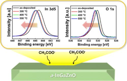
在器件制造过程中,控制非晶氧化半导体InGaZnO (IGZO)薄膜中的氧空位(VO),或者更准确地说是局部氧缺乏,是至关重要的,因为它会影响薄膜晶体管(TFT)器件的传输特性和可靠性。在x射线光电子能谱(XPS)中测量o1s峰并进行峰反卷积已被广泛用于识别VO状态,其中反卷积的结合能(BE)在531 ~ 532 eV之间的o1s峰被认为代表VO状态。然而,这项工作表明,In 3d5/2峰是VO(或载流子)浓度的更可靠的指标,其中较高的In 3d5/2峰BE对应于较低的VO浓度和较高的TFT阈值电压。531 ~ 532 eV BE的o1s峰不是来自IGZO膜内VO附近的氧离子,而是来自表面乙酸分子中的氧原子。当IGZO表面被空气中的OH和CO2污染时,形成了更多的醋酸盐,增加了峰值强度。此外,这种吸附在具有弱金属-氧键的材料中更为普遍。值得注意的是,当在XPS室中原位溅射清洗IGZO膜表面的醋酸盐时,531-532 eV BE的o1s峰消失。
Identifying the Chemical Structure of Indium–Gallium–Zinc Oxide Thin Films with Oxygen Vacancy Variation
Controlling the oxygen vacancy (VO), or more precisely, the local oxygen deficiency, in amorphous oxide semiconductor InGaZnO (IGZO) thin films during device fabrication is crucial because it affects the transfer characteristics and reliability of thin-film transistor (TFT) devices. Measuring the O 1s peak in X-ray photoelectron spectroscopy (XPS) and performing peak deconvolution have been widely used to identify the VO status, where the deconvoluted O 1s peak with a binding energy (BE) between 531 and 532 eV is considered to represent VO. However, this work reveals that the In 3d5/2 peak is a more reliable indicator of the VO (or carrier) concentration, where a higher In 3d5/2 peak BE corresponds to a lower VO concentration and higher TFT threshold voltages. The O 1s peak at 531–532 eV BE did not originate from the oxygen ions near the VO inside the IGZO film but rather from the oxygen atoms in the acetate molecules on the surface. When the IGZO surface was contaminated by OH and CO2 from the air, more acetate was formed, increasing the peak intensity. Moreover, such adsorption was more prevalent in materials exhibiting weak metal–oxygen bonds. Notably, the O 1s peak at 531–532 eV BE disappeared when the acetate on the IGZO film surface was in situ sputter-cleaned in the XPS chamber.
期刊介绍:
ACS Applied Electronic Materials is an interdisciplinary journal publishing original research covering all aspects of electronic materials. The journal is devoted to reports of new and original experimental and theoretical research of an applied nature that integrate knowledge in the areas of materials science, engineering, optics, physics, and chemistry into important applications of electronic materials. Sample research topics that span the journal's scope are inorganic, organic, ionic and polymeric materials with properties that include conducting, semiconducting, superconducting, insulating, dielectric, magnetic, optoelectronic, piezoelectric, ferroelectric and thermoelectric.
Indexed/Abstracted:
Web of Science SCIE
Scopus
CAS
INSPEC
Portico

 求助内容:
求助内容: 应助结果提醒方式:


