{"title":"通过晶圆键合辅助转移制造芯片级二维单层单晶。","authors":"Wenjing Wu, , , Shisong Luo, , , Tao Li, , , Enzi Zhai, , , Ziyang Wang, , , Xinyan Li, , , Yimo Han, , , Yuxuan Cosmi Lin, , , Yuji Zhao, , , Junichiro Kono, , and , Shengxi Huang*, ","doi":"10.1021/acs.nanolett.5c03755","DOIUrl":null,"url":null,"abstract":"<p >Significant progress has been made in growing large-area transition metal dichalcogenide (TMD) monolayers, but most rely on stitching small flakes, which can affect electronic and optical performance. High-quality single-crystal monolayers are needed for device applications. Here, we report a wafer-bonder-assisted transfer (WBAT) method to produce uniform, crack-free, single-crystal TMD monolayers over large areas. This technique integrates gold-tape exfoliation with wafer-scale bonding, enabling flake sizes over 10<sup>6</sup> times larger than those from traditional Scotch tape exfoliation. Compared to hand-press transfer, WBAT yields higher-quality monolayers with fewer cracks, reduced strain, and over 2-fold improvement in photoluminescence uniformity, as confirmed by Raman and PL mapping. Fabricated field-effect transistor arrays show high mobility and on–off ratio. The WBAT method offers high yield, reproducibility, and compatibility with various 2D materials, heterostructures, and substrates, aligning with standard semiconductor processes. It provides a scalable solution for integrating high-quality TMD monolayers into next-generation electronic and optoelectronic devices.</p>","PeriodicalId":53,"journal":{"name":"Nano Letters","volume":"25 39","pages":"14395–14403"},"PeriodicalIF":9.1000,"publicationDate":"2025-09-23","publicationTypes":"Journal Article","fieldsOfStudy":null,"isOpenAccess":false,"openAccessPdf":"","citationCount":"0","resultStr":"{\"title\":\"Manufacturing Chip-Scale 2D Monolayer Single Crystals through Wafer-Bonder-Assisted Transfer\",\"authors\":\"Wenjing Wu, , , Shisong Luo, , , Tao Li, , , Enzi Zhai, , , Ziyang Wang, , , Xinyan Li, , , Yimo Han, , , Yuxuan Cosmi Lin, , , Yuji Zhao, , , Junichiro Kono, , and , Shengxi Huang*, \",\"doi\":\"10.1021/acs.nanolett.5c03755\",\"DOIUrl\":null,\"url\":null,\"abstract\":\"<p >Significant progress has been made in growing large-area transition metal dichalcogenide (TMD) monolayers, but most rely on stitching small flakes, which can affect electronic and optical performance. High-quality single-crystal monolayers are needed for device applications. Here, we report a wafer-bonder-assisted transfer (WBAT) method to produce uniform, crack-free, single-crystal TMD monolayers over large areas. This technique integrates gold-tape exfoliation with wafer-scale bonding, enabling flake sizes over 10<sup>6</sup> times larger than those from traditional Scotch tape exfoliation. Compared to hand-press transfer, WBAT yields higher-quality monolayers with fewer cracks, reduced strain, and over 2-fold improvement in photoluminescence uniformity, as confirmed by Raman and PL mapping. Fabricated field-effect transistor arrays show high mobility and on–off ratio. The WBAT method offers high yield, reproducibility, and compatibility with various 2D materials, heterostructures, and substrates, aligning with standard semiconductor processes. It provides a scalable solution for integrating high-quality TMD monolayers into next-generation electronic and optoelectronic devices.</p>\",\"PeriodicalId\":53,\"journal\":{\"name\":\"Nano Letters\",\"volume\":\"25 39\",\"pages\":\"14395–14403\"},\"PeriodicalIF\":9.1000,\"publicationDate\":\"2025-09-23\",\"publicationTypes\":\"Journal Article\",\"fieldsOfStudy\":null,\"isOpenAccess\":false,\"openAccessPdf\":\"\",\"citationCount\":\"0\",\"resultStr\":null,\"platform\":\"Semanticscholar\",\"paperid\":null,\"PeriodicalName\":\"Nano Letters\",\"FirstCategoryId\":\"88\",\"ListUrlMain\":\"https://pubs.acs.org/doi/10.1021/acs.nanolett.5c03755\",\"RegionNum\":1,\"RegionCategory\":\"材料科学\",\"ArticlePicture\":[],\"TitleCN\":null,\"AbstractTextCN\":null,\"PMCID\":null,\"EPubDate\":\"\",\"PubModel\":\"\",\"JCR\":\"Q1\",\"JCRName\":\"CHEMISTRY, MULTIDISCIPLINARY\",\"Score\":null,\"Total\":0}","platform":"Semanticscholar","paperid":null,"PeriodicalName":"Nano Letters","FirstCategoryId":"88","ListUrlMain":"https://pubs.acs.org/doi/10.1021/acs.nanolett.5c03755","RegionNum":1,"RegionCategory":"材料科学","ArticlePicture":[],"TitleCN":null,"AbstractTextCN":null,"PMCID":null,"EPubDate":"","PubModel":"","JCR":"Q1","JCRName":"CHEMISTRY, MULTIDISCIPLINARY","Score":null,"Total":0}
Manufacturing Chip-Scale 2D Monolayer Single Crystals through Wafer-Bonder-Assisted Transfer
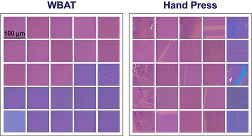
Significant progress has been made in growing large-area transition metal dichalcogenide (TMD) monolayers, but most rely on stitching small flakes, which can affect electronic and optical performance. High-quality single-crystal monolayers are needed for device applications. Here, we report a wafer-bonder-assisted transfer (WBAT) method to produce uniform, crack-free, single-crystal TMD monolayers over large areas. This technique integrates gold-tape exfoliation with wafer-scale bonding, enabling flake sizes over 106 times larger than those from traditional Scotch tape exfoliation. Compared to hand-press transfer, WBAT yields higher-quality monolayers with fewer cracks, reduced strain, and over 2-fold improvement in photoluminescence uniformity, as confirmed by Raman and PL mapping. Fabricated field-effect transistor arrays show high mobility and on–off ratio. The WBAT method offers high yield, reproducibility, and compatibility with various 2D materials, heterostructures, and substrates, aligning with standard semiconductor processes. It provides a scalable solution for integrating high-quality TMD monolayers into next-generation electronic and optoelectronic devices.
期刊介绍:
Nano Letters serves as a dynamic platform for promptly disseminating original results in fundamental, applied, and emerging research across all facets of nanoscience and nanotechnology. A pivotal criterion for inclusion within Nano Letters is the convergence of at least two different areas or disciplines, ensuring a rich interdisciplinary scope. The journal is dedicated to fostering exploration in diverse areas, including:
- Experimental and theoretical findings on physical, chemical, and biological phenomena at the nanoscale
- Synthesis, characterization, and processing of organic, inorganic, polymer, and hybrid nanomaterials through physical, chemical, and biological methodologies
- Modeling and simulation of synthetic, assembly, and interaction processes
- Realization of integrated nanostructures and nano-engineered devices exhibiting advanced performance
- Applications of nanoscale materials in living and environmental systems
Nano Letters is committed to advancing and showcasing groundbreaking research that intersects various domains, fostering innovation and collaboration in the ever-evolving field of nanoscience and nanotechnology.

 求助内容:
求助内容: 应助结果提醒方式:


