Sangyeon Pak, , , John Hong*, , and , SeungNam Cha*,
{"title":"二维电子学的最新接触策略","authors":"Sangyeon Pak, , , John Hong*, , and , SeungNam Cha*, ","doi":"10.1021/acsnano.5c07026","DOIUrl":null,"url":null,"abstract":"<p >Two-dimensional (2D) semiconductors such as monolayer MoS<sub>2</sub> and WSe<sub>2</sub> have rapidly gained attention as next-generation channel materials for ultrascaled electronics owing to their exceptional electrostatic control and atomic-scale thickness. Despite their promise, the high contact resistance and Fermi-level pinning at the metal–semiconductor interface continue to hinder optimal device performance and scalability. This review highlights recent breakthroughs in contact engineering─including van der Waals metal transfer, semimetallic and edge contacts, contact doping, strain engineering, and self-healing electrodes─that collectively enhance carrier injection, reduce Schottky barriers, and improve interface stability. We also examine complementary metal-oxide semiconductor-compatible integration strategies and the growing role of computational screening and machine learning in accelerating the discovery of optimal contact materials. These advances have enabled record-setting 2D field-effect transistor performance at sub-50 nm gate lengths, underscoring the increasing readiness of 2D materials for high-volume, energy-efficient applications beyond the silicon era.</p>","PeriodicalId":21,"journal":{"name":"ACS Nano","volume":"19 39","pages":"34449–34468"},"PeriodicalIF":16.0000,"publicationDate":"2025-09-23","publicationTypes":"Journal Article","fieldsOfStudy":null,"isOpenAccess":false,"openAccessPdf":"","citationCount":"0","resultStr":"{\"title\":\"Recent Contact Strategies for Two-Dimensional Electronics\",\"authors\":\"Sangyeon Pak, , , John Hong*, , and , SeungNam Cha*, \",\"doi\":\"10.1021/acsnano.5c07026\",\"DOIUrl\":null,\"url\":null,\"abstract\":\"<p >Two-dimensional (2D) semiconductors such as monolayer MoS<sub>2</sub> and WSe<sub>2</sub> have rapidly gained attention as next-generation channel materials for ultrascaled electronics owing to their exceptional electrostatic control and atomic-scale thickness. Despite their promise, the high contact resistance and Fermi-level pinning at the metal–semiconductor interface continue to hinder optimal device performance and scalability. This review highlights recent breakthroughs in contact engineering─including van der Waals metal transfer, semimetallic and edge contacts, contact doping, strain engineering, and self-healing electrodes─that collectively enhance carrier injection, reduce Schottky barriers, and improve interface stability. We also examine complementary metal-oxide semiconductor-compatible integration strategies and the growing role of computational screening and machine learning in accelerating the discovery of optimal contact materials. These advances have enabled record-setting 2D field-effect transistor performance at sub-50 nm gate lengths, underscoring the increasing readiness of 2D materials for high-volume, energy-efficient applications beyond the silicon era.</p>\",\"PeriodicalId\":21,\"journal\":{\"name\":\"ACS Nano\",\"volume\":\"19 39\",\"pages\":\"34449–34468\"},\"PeriodicalIF\":16.0000,\"publicationDate\":\"2025-09-23\",\"publicationTypes\":\"Journal Article\",\"fieldsOfStudy\":null,\"isOpenAccess\":false,\"openAccessPdf\":\"\",\"citationCount\":\"0\",\"resultStr\":null,\"platform\":\"Semanticscholar\",\"paperid\":null,\"PeriodicalName\":\"ACS Nano\",\"FirstCategoryId\":\"88\",\"ListUrlMain\":\"https://pubs.acs.org/doi/10.1021/acsnano.5c07026\",\"RegionNum\":1,\"RegionCategory\":\"材料科学\",\"ArticlePicture\":[],\"TitleCN\":null,\"AbstractTextCN\":null,\"PMCID\":null,\"EPubDate\":\"\",\"PubModel\":\"\",\"JCR\":\"Q1\",\"JCRName\":\"CHEMISTRY, MULTIDISCIPLINARY\",\"Score\":null,\"Total\":0}","platform":"Semanticscholar","paperid":null,"PeriodicalName":"ACS Nano","FirstCategoryId":"88","ListUrlMain":"https://pubs.acs.org/doi/10.1021/acsnano.5c07026","RegionNum":1,"RegionCategory":"材料科学","ArticlePicture":[],"TitleCN":null,"AbstractTextCN":null,"PMCID":null,"EPubDate":"","PubModel":"","JCR":"Q1","JCRName":"CHEMISTRY, MULTIDISCIPLINARY","Score":null,"Total":0}
Recent Contact Strategies for Two-Dimensional Electronics
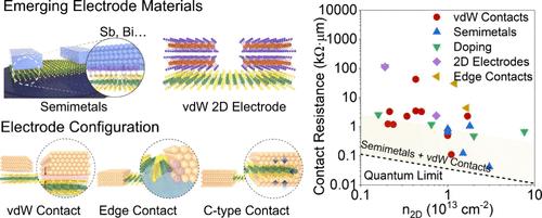
Two-dimensional (2D) semiconductors such as monolayer MoS2 and WSe2 have rapidly gained attention as next-generation channel materials for ultrascaled electronics owing to their exceptional electrostatic control and atomic-scale thickness. Despite their promise, the high contact resistance and Fermi-level pinning at the metal–semiconductor interface continue to hinder optimal device performance and scalability. This review highlights recent breakthroughs in contact engineering─including van der Waals metal transfer, semimetallic and edge contacts, contact doping, strain engineering, and self-healing electrodes─that collectively enhance carrier injection, reduce Schottky barriers, and improve interface stability. We also examine complementary metal-oxide semiconductor-compatible integration strategies and the growing role of computational screening and machine learning in accelerating the discovery of optimal contact materials. These advances have enabled record-setting 2D field-effect transistor performance at sub-50 nm gate lengths, underscoring the increasing readiness of 2D materials for high-volume, energy-efficient applications beyond the silicon era.
期刊介绍:
ACS Nano, published monthly, serves as an international forum for comprehensive articles on nanoscience and nanotechnology research at the intersections of chemistry, biology, materials science, physics, and engineering. The journal fosters communication among scientists in these communities, facilitating collaboration, new research opportunities, and advancements through discoveries. ACS Nano covers synthesis, assembly, characterization, theory, and simulation of nanostructures, nanobiotechnology, nanofabrication, methods and tools for nanoscience and nanotechnology, and self- and directed-assembly. Alongside original research articles, it offers thorough reviews, perspectives on cutting-edge research, and discussions envisioning the future of nanoscience and nanotechnology.


 求助内容:
求助内容: 应助结果提醒方式:


