Jaebum Jeong , Gun woong Kim , Eun Jin Park , Seong Woo Jeong , Seok Hwan Jang , Jae Yeong Jeong , Soo Won Heo , Jun Young Kim
{"title":"低温电子束退火提高有机光电探测器的性能","authors":"Jaebum Jeong , Gun woong Kim , Eun Jin Park , Seong Woo Jeong , Seok Hwan Jang , Jae Yeong Jeong , Soo Won Heo , Jun Young Kim","doi":"10.1016/j.matdes.2025.114778","DOIUrl":null,"url":null,"abstract":"<div><div>Organic photodetectors (OPDs) are promising candidates for next-generation optoelectronic devices due to their flexibility, low cost, and scalability. Enhancing OPD performance requires optimizing key layers such as the electron transport layer (ETL) using low-temperature processes to prevent thermal degradation. This study explores the use of low-temperature electron beam annealing (EBA) to improve the performance of Al-doped ZnO (AZO)-based ETLs. The impact of EBA irradiation time (1–8 min) on the structural, morphological, and electrical properties of AZO films was systematically analyzed. EBA effectively modulated oxygen vacancies and reduced surface roughness, lowering trap density and leakage current while enhancing charge transport. An OPD with an ETL treated by 8 min of EBA exhibited superior detectivity (2.22 × 10<sup>13</sup> Jones at 0 V) and significantly reduced leakage current compared to a device with conventionally annealed ETLs. Importantly, the low-temperature EBA process preserved the amorphous state of AZO, making it suitable for heat-sensitive and flexible substrates. These findings demonstrate that EBA is a powerful, scalable method for ETL optimization in OPDs and offers a pathway toward high-performance, energy-efficient, and flexible optoelectronic devices.</div></div>","PeriodicalId":383,"journal":{"name":"Materials & Design","volume":"259 ","pages":"Article 114778"},"PeriodicalIF":7.9000,"publicationDate":"2025-09-15","publicationTypes":"Journal Article","fieldsOfStudy":null,"isOpenAccess":false,"openAccessPdf":"","citationCount":"0","resultStr":"{\"title\":\"Improving the performance of organic photodetectors by low-temperature electron beam annealing\",\"authors\":\"Jaebum Jeong , Gun woong Kim , Eun Jin Park , Seong Woo Jeong , Seok Hwan Jang , Jae Yeong Jeong , Soo Won Heo , Jun Young Kim\",\"doi\":\"10.1016/j.matdes.2025.114778\",\"DOIUrl\":null,\"url\":null,\"abstract\":\"<div><div>Organic photodetectors (OPDs) are promising candidates for next-generation optoelectronic devices due to their flexibility, low cost, and scalability. Enhancing OPD performance requires optimizing key layers such as the electron transport layer (ETL) using low-temperature processes to prevent thermal degradation. This study explores the use of low-temperature electron beam annealing (EBA) to improve the performance of Al-doped ZnO (AZO)-based ETLs. The impact of EBA irradiation time (1–8 min) on the structural, morphological, and electrical properties of AZO films was systematically analyzed. EBA effectively modulated oxygen vacancies and reduced surface roughness, lowering trap density and leakage current while enhancing charge transport. An OPD with an ETL treated by 8 min of EBA exhibited superior detectivity (2.22 × 10<sup>13</sup> Jones at 0 V) and significantly reduced leakage current compared to a device with conventionally annealed ETLs. Importantly, the low-temperature EBA process preserved the amorphous state of AZO, making it suitable for heat-sensitive and flexible substrates. These findings demonstrate that EBA is a powerful, scalable method for ETL optimization in OPDs and offers a pathway toward high-performance, energy-efficient, and flexible optoelectronic devices.</div></div>\",\"PeriodicalId\":383,\"journal\":{\"name\":\"Materials & Design\",\"volume\":\"259 \",\"pages\":\"Article 114778\"},\"PeriodicalIF\":7.9000,\"publicationDate\":\"2025-09-15\",\"publicationTypes\":\"Journal Article\",\"fieldsOfStudy\":null,\"isOpenAccess\":false,\"openAccessPdf\":\"\",\"citationCount\":\"0\",\"resultStr\":null,\"platform\":\"Semanticscholar\",\"paperid\":null,\"PeriodicalName\":\"Materials & Design\",\"FirstCategoryId\":\"88\",\"ListUrlMain\":\"https://www.sciencedirect.com/science/article/pii/S0264127525011980\",\"RegionNum\":2,\"RegionCategory\":\"材料科学\",\"ArticlePicture\":[],\"TitleCN\":null,\"AbstractTextCN\":null,\"PMCID\":null,\"EPubDate\":\"\",\"PubModel\":\"\",\"JCR\":\"Q1\",\"JCRName\":\"MATERIALS SCIENCE, MULTIDISCIPLINARY\",\"Score\":null,\"Total\":0}","platform":"Semanticscholar","paperid":null,"PeriodicalName":"Materials & Design","FirstCategoryId":"88","ListUrlMain":"https://www.sciencedirect.com/science/article/pii/S0264127525011980","RegionNum":2,"RegionCategory":"材料科学","ArticlePicture":[],"TitleCN":null,"AbstractTextCN":null,"PMCID":null,"EPubDate":"","PubModel":"","JCR":"Q1","JCRName":"MATERIALS SCIENCE, MULTIDISCIPLINARY","Score":null,"Total":0}
Improving the performance of organic photodetectors by low-temperature electron beam annealing
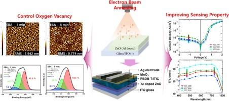
Organic photodetectors (OPDs) are promising candidates for next-generation optoelectronic devices due to their flexibility, low cost, and scalability. Enhancing OPD performance requires optimizing key layers such as the electron transport layer (ETL) using low-temperature processes to prevent thermal degradation. This study explores the use of low-temperature electron beam annealing (EBA) to improve the performance of Al-doped ZnO (AZO)-based ETLs. The impact of EBA irradiation time (1–8 min) on the structural, morphological, and electrical properties of AZO films was systematically analyzed. EBA effectively modulated oxygen vacancies and reduced surface roughness, lowering trap density and leakage current while enhancing charge transport. An OPD with an ETL treated by 8 min of EBA exhibited superior detectivity (2.22 × 10¹³ Jones at 0 V) and significantly reduced leakage current compared to a device with conventionally annealed ETLs. Importantly, the low-temperature EBA process preserved the amorphous state of AZO, making it suitable for heat-sensitive and flexible substrates. These findings demonstrate that EBA is a powerful, scalable method for ETL optimization in OPDs and offers a pathway toward high-performance, energy-efficient, and flexible optoelectronic devices.
期刊介绍:
Materials and Design is a multi-disciplinary journal that publishes original research reports, review articles, and express communications. The journal focuses on studying the structure and properties of inorganic and organic materials, advancements in synthesis, processing, characterization, and testing, the design of materials and engineering systems, and their applications in technology. It aims to bring together various aspects of materials science, engineering, physics, and chemistry.
The journal explores themes ranging from materials to design and aims to reveal the connections between natural and artificial materials, as well as experiment and modeling. Manuscripts submitted to Materials and Design should contain elements of discovery and surprise, as they often contribute new insights into the architecture and function of matter.