高纵横比(AR)纳米尺度tsv的新型铜填充方法

IF 3.1 4区 工程技术 Q2 ENGINEERING, ELECTRICAL & ELECTRONIC
Han Jiang , Yang Wang , Ziyu Liu , Yabin Sun , Qingqing Sun , David Wei Zhang
{"title":"高纵横比(AR)纳米尺度tsv的新型铜填充方法","authors":"Han Jiang ,&nbsp;Yang Wang ,&nbsp;Ziyu Liu ,&nbsp;Yabin Sun ,&nbsp;Qingqing Sun ,&nbsp;David Wei Zhang","doi":"10.1016/j.mee.2025.112417","DOIUrl":null,"url":null,"abstract":"<div><div>Nano-scale through‑silicon vias (n-TSVs) plays the key role in connecting the active front-side of devices and the backside power delivery network (BS-PDN) in the three-dimensional integrated circuit (3D IC). High-quality Cu filling is the most important in the n-TSVs fabrication. As the diameter decreases and the aspect ratio (AR) increases, the challenges associated with seed layer deposition, surface pre-wetting, and electrochemical deposition (ECD) will intensify. In this study, the electron beam induced deposition (EBID) method has been first proposed to deposit the seed layer for high-AR n-TSVs. Additionally, isopropanol pre-wetting is proposed to enhance surface wettability, thereby eliminating air bubbles within the via and ensuring complete filling of the electrolyte. Finally, the effect of electrolyte additives and current density on the ECD process have also been extensively investigated. The thickness of seed layer deposited by EBID exhibits high step coverage, uniformity and continuity at the top and the bottom of via. Meanwhile, the wettability of seed layer surface treated by isopropanol has been greatly increased. During the ECD process, the deposition rate of Cu is main affected by the suppressor. Besides, the current density should be chosen within a moderate value (≥ 0.03 A/dm<sup>2</sup> and ≤ 0.3 A/dm<sup>2</sup>), which can increase the deposition rate and avoid the premature closing of the via opening. With the optimized processes above, the n-TSVs of Type-I (440-nm-diameter and 4.81:1-AR) and Type-II (150-nm-diameter and 9.25:1-AR) have been conformally filled without voids and breaks.</div></div>","PeriodicalId":18557,"journal":{"name":"Microelectronic Engineering","volume":"302 ","pages":"Article 112417"},"PeriodicalIF":3.1000,"publicationDate":"2025-09-11","publicationTypes":"Journal Article","fieldsOfStudy":null,"isOpenAccess":false,"openAccessPdf":"","citationCount":"0","resultStr":"{\"title\":\"A novel cu filling method for high-aspect-ratio (AR) nano-scale TSVs\",\"authors\":\"Han Jiang ,&nbsp;Yang Wang ,&nbsp;Ziyu Liu ,&nbsp;Yabin Sun ,&nbsp;Qingqing Sun ,&nbsp;David Wei Zhang\",\"doi\":\"10.1016/j.mee.2025.112417\",\"DOIUrl\":null,\"url\":null,\"abstract\":\"<div><div>Nano-scale through‑silicon vias (n-TSVs) plays the key role in connecting the active front-side of devices and the backside power delivery network (BS-PDN) in the three-dimensional integrated circuit (3D IC). High-quality Cu filling is the most important in the n-TSVs fabrication. As the diameter decreases and the aspect ratio (AR) increases, the challenges associated with seed layer deposition, surface pre-wetting, and electrochemical deposition (ECD) will intensify. In this study, the electron beam induced deposition (EBID) method has been first proposed to deposit the seed layer for high-AR n-TSVs. Additionally, isopropanol pre-wetting is proposed to enhance surface wettability, thereby eliminating air bubbles within the via and ensuring complete filling of the electrolyte. Finally, the effect of electrolyte additives and current density on the ECD process have also been extensively investigated. The thickness of seed layer deposited by EBID exhibits high step coverage, uniformity and continuity at the top and the bottom of via. Meanwhile, the wettability of seed layer surface treated by isopropanol has been greatly increased. During the ECD process, the deposition rate of Cu is main affected by the suppressor. Besides, the current density should be chosen within a moderate value (≥ 0.03 A/dm<sup>2</sup> and ≤ 0.3 A/dm<sup>2</sup>), which can increase the deposition rate and avoid the premature closing of the via opening. With the optimized processes above, the n-TSVs of Type-I (440-nm-diameter and 4.81:1-AR) and Type-II (150-nm-diameter and 9.25:1-AR) have been conformally filled without voids and breaks.</div></div>\",\"PeriodicalId\":18557,\"journal\":{\"name\":\"Microelectronic Engineering\",\"volume\":\"302 \",\"pages\":\"Article 112417\"},\"PeriodicalIF\":3.1000,\"publicationDate\":\"2025-09-11\",\"publicationTypes\":\"Journal Article\",\"fieldsOfStudy\":null,\"isOpenAccess\":false,\"openAccessPdf\":\"\",\"citationCount\":\"0\",\"resultStr\":null,\"platform\":\"Semanticscholar\",\"paperid\":null,\"PeriodicalName\":\"Microelectronic Engineering\",\"FirstCategoryId\":\"5\",\"ListUrlMain\":\"https://www.sciencedirect.com/science/article/pii/S0167931725001066\",\"RegionNum\":4,\"RegionCategory\":\"工程技术\",\"ArticlePicture\":[],\"TitleCN\":null,\"AbstractTextCN\":null,\"PMCID\":null,\"EPubDate\":\"\",\"PubModel\":\"\",\"JCR\":\"Q2\",\"JCRName\":\"ENGINEERING, ELECTRICAL & ELECTRONIC\",\"Score\":null,\"Total\":0}","platform":"Semanticscholar","paperid":null,"PeriodicalName":"Microelectronic Engineering","FirstCategoryId":"5","ListUrlMain":"https://www.sciencedirect.com/science/article/pii/S0167931725001066","RegionNum":4,"RegionCategory":"工程技术","ArticlePicture":[],"TitleCN":null,"AbstractTextCN":null,"PMCID":null,"EPubDate":"","PubModel":"","JCR":"Q2","JCRName":"ENGINEERING, ELECTRICAL & ELECTRONIC","Score":null,"Total":0}
引用次数: 0

摘要

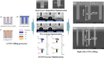
在三维集成电路(3D IC)中,纳米级硅通孔(n- tsv)在连接器件的有源前端和背面电力输送网络(BS-PDN)方面起着关键作用。高质量的Cu填充是n- tsv制备中最重要的环节。随着直径的减小和宽高比(AR)的增加,与种子层沉积、表面预润湿和电化学沉积(ECD)相关的挑战将会加剧。在本研究中,首次提出了电子束诱导沉积(EBID)方法沉积高ar n- tsv的种子层。此外,异丙醇预湿可以提高表面润湿性,从而消除通孔内的气泡,确保电解质完全填充。最后,电解质添加剂和电流密度对ECD过程的影响也得到了广泛的研究。EBID沉积的种子层厚度具有较高的台阶覆盖度、均匀性和孔道顶部和底部的连续性。同时,异丙醇处理后种子层表面的润湿性大大提高。在ECD过程中,铜的沉积速率主要受抑制因子的影响。电流密度应选择在一个适中的范围内(≥0.03 a /dm2和≤0.3 a /dm2),这样可以提高沉积速率,避免过孔过早闭合。通过上述优化工艺,i型(440-nm直径,4.81:1-AR)和ii型(150-nm直径,9.25:1-AR)的n- tsv均得到了保形填充,无空洞和断裂。
本文章由计算机程序翻译,如有差异,请以英文原文为准。

A novel cu filling method for high-aspect-ratio (AR) nano-scale TSVs

A novel cu filling method for high-aspect-ratio (AR) nano-scale TSVs
Nano-scale through‑silicon vias (n-TSVs) plays the key role in connecting the active front-side of devices and the backside power delivery network (BS-PDN) in the three-dimensional integrated circuit (3D IC). High-quality Cu filling is the most important in the n-TSVs fabrication. As the diameter decreases and the aspect ratio (AR) increases, the challenges associated with seed layer deposition, surface pre-wetting, and electrochemical deposition (ECD) will intensify. In this study, the electron beam induced deposition (EBID) method has been first proposed to deposit the seed layer for high-AR n-TSVs. Additionally, isopropanol pre-wetting is proposed to enhance surface wettability, thereby eliminating air bubbles within the via and ensuring complete filling of the electrolyte. Finally, the effect of electrolyte additives and current density on the ECD process have also been extensively investigated. The thickness of seed layer deposited by EBID exhibits high step coverage, uniformity and continuity at the top and the bottom of via. Meanwhile, the wettability of seed layer surface treated by isopropanol has been greatly increased. During the ECD process, the deposition rate of Cu is main affected by the suppressor. Besides, the current density should be chosen within a moderate value (≥ 0.03 A/dm2 and ≤ 0.3 A/dm2), which can increase the deposition rate and avoid the premature closing of the via opening. With the optimized processes above, the n-TSVs of Type-I (440-nm-diameter and 4.81:1-AR) and Type-II (150-nm-diameter and 9.25:1-AR) have been conformally filled without voids and breaks.
求助全文
通过发布文献求助,成功后即可免费获取论文全文。 去求助
来源期刊
Microelectronic Engineering
Microelectronic Engineering 工程技术-工程:电子与电气
CiteScore
5.30
自引率
4.30%
发文量
131
审稿时长
29 days
期刊介绍: Microelectronic Engineering is the premier nanoprocessing, and nanotechnology journal focusing on fabrication of electronic, photonic, bioelectronic, electromechanic and fluidic devices and systems, and their applications in the broad areas of electronics, photonics, energy, life sciences, and environment. It covers also the expanding interdisciplinary field of "more than Moore" and "beyond Moore" integrated nanoelectronics / photonics and micro-/nano-/bio-systems. Through its unique mixture of peer-reviewed articles, reviews, accelerated publications, short and Technical notes, and the latest research news on key developments, Microelectronic Engineering provides comprehensive coverage of this exciting, interdisciplinary and dynamic new field for researchers in academia and professionals in industry.
×
引用
GB/T 7714-2015
复制
MLA
复制
APA
复制
导出至
BibTeX EndNote RefMan NoteFirst NoteExpress
×
提示
您的信息不完整,为了账户安全,请先补充。
现在去补充
×
提示
您因"违规操作"
具体请查看互助需知
我知道了
×
提示
确定
请完成安全验证×
copy
已复制链接
快去分享给好友吧!
我知道了
右上角分享
点击右上角分享
0
联系我们:info@booksci.cn Book学术提供免费学术资源搜索服务,方便国内外学者检索中英文文献。致力于提供最便捷和优质的服务体验。 Copyright © 2023 布克学术 All rights reserved.
京ICP备2023020795号-1
ghs 京公网安备 11010802042870号
Book学术文献互助
Book学术文献互助群
群 号:604180095
Book学术官方微信