L. N. Maskaeva, A. V. Pozdin, E. V. Mostovshchikova, V. F. Markov, O. S. Eltsov, V. I. Voronin, I. V. Baklanova, P. N. Mushnikov
{"title":"低温一锅法合成镍碘掺杂硫化铅光敏薄膜","authors":"L. N. Maskaeva, A. V. Pozdin, E. V. Mostovshchikova, V. F. Markov, O. S. Eltsov, V. I. Voronin, I. V. Baklanova, P. N. Mushnikov","doi":"10.1007/s10854-025-15816-6","DOIUrl":null,"url":null,"abstract":"<div><p>The efficiency of combined donor–acceptor doping of thin lead sulfide films with nickel and iodine ions using the <i>one-po</i>t approach for obtaining photosensitive lead sulfide layers PbS(I, Ni) was shown. Chemical bath deposition of the lead sulfide films from an ammonia-citrate reaction mixture with a combined additive of NH<sub>4</sub>I and NiCl<sub>2</sub> was carried. The conditions for the films deposition were preliminarily determined by analyzing ionic equilibria in an ammonia-citrate reaction mixture. Composition, morphology and structure of the synthesized layers were studied using scanning electron microscopy, energy-dispersive elemental analysis and X-ray diffraction. Non-monotonic changes of the content of the main elements Pb, S, I, and Ni in the lead sulfide films, lattice parameter, crystallographic orientation of grains, microstresses and coherent scattering regions, as well as band gap depending on the concentration of NiCl<sub>2</sub> in the reaction bath with extreme values near 1–2 mM NiCl<sub>2</sub> were revealed. The analysis of Raman and Fourier-transform infrared transmission spectra showed the formation of diiodine pentoxide I<sub>2</sub>O<sub>5</sub>, iodate ion IO<sup>3−</sup>, and nickel oxide NiO in the PbS(I, Ni) films in addition to the PbI<sub>2</sub> phase. A 1.8-fold increase in voltage sensitivity and a 7.5-fold increase in detectivity of the PbS(I, Ni) film deposited in the presence of 0.15 M NH<sub>4</sub>I and 2 mM NiCl<sub>2</sub> compared to the film deposited in the presence of only 0.15 M NH<sub>4</sub>I were found. A significant increase in voltage sensitivity and detectivity of the PbS(I, Ni) films is caused by a synergistic effect of the doping additives with the formation of photoactive phases of lead iodide and iodine and nickel oxides.</p></div>","PeriodicalId":646,"journal":{"name":"Journal of Materials Science: Materials in Electronics","volume":"36 26","pages":""},"PeriodicalIF":2.8000,"publicationDate":"2025-09-20","publicationTypes":"Journal Article","fieldsOfStudy":null,"isOpenAccess":false,"openAccessPdf":"","citationCount":"0","resultStr":"{\"title\":\"Low-temperature one-pot synthesis of nickel and iodine-doped photosensitive thin films of lead(II) sulfide\",\"authors\":\"L. N. Maskaeva, A. V. Pozdin, E. V. Mostovshchikova, V. F. Markov, O. S. Eltsov, V. I. Voronin, I. V. Baklanova, P. N. Mushnikov\",\"doi\":\"10.1007/s10854-025-15816-6\",\"DOIUrl\":null,\"url\":null,\"abstract\":\"<div><p>The efficiency of combined donor–acceptor doping of thin lead sulfide films with nickel and iodine ions using the <i>one-po</i>t approach for obtaining photosensitive lead sulfide layers PbS(I, Ni) was shown. Chemical bath deposition of the lead sulfide films from an ammonia-citrate reaction mixture with a combined additive of NH<sub>4</sub>I and NiCl<sub>2</sub> was carried. The conditions for the films deposition were preliminarily determined by analyzing ionic equilibria in an ammonia-citrate reaction mixture. Composition, morphology and structure of the synthesized layers were studied using scanning electron microscopy, energy-dispersive elemental analysis and X-ray diffraction. Non-monotonic changes of the content of the main elements Pb, S, I, and Ni in the lead sulfide films, lattice parameter, crystallographic orientation of grains, microstresses and coherent scattering regions, as well as band gap depending on the concentration of NiCl<sub>2</sub> in the reaction bath with extreme values near 1–2 mM NiCl<sub>2</sub> were revealed. The analysis of Raman and Fourier-transform infrared transmission spectra showed the formation of diiodine pentoxide I<sub>2</sub>O<sub>5</sub>, iodate ion IO<sup>3−</sup>, and nickel oxide NiO in the PbS(I, Ni) films in addition to the PbI<sub>2</sub> phase. A 1.8-fold increase in voltage sensitivity and a 7.5-fold increase in detectivity of the PbS(I, Ni) film deposited in the presence of 0.15 M NH<sub>4</sub>I and 2 mM NiCl<sub>2</sub> compared to the film deposited in the presence of only 0.15 M NH<sub>4</sub>I were found. A significant increase in voltage sensitivity and detectivity of the PbS(I, Ni) films is caused by a synergistic effect of the doping additives with the formation of photoactive phases of lead iodide and iodine and nickel oxides.</p></div>\",\"PeriodicalId\":646,\"journal\":{\"name\":\"Journal of Materials Science: Materials in Electronics\",\"volume\":\"36 26\",\"pages\":\"\"},\"PeriodicalIF\":2.8000,\"publicationDate\":\"2025-09-20\",\"publicationTypes\":\"Journal Article\",\"fieldsOfStudy\":null,\"isOpenAccess\":false,\"openAccessPdf\":\"\",\"citationCount\":\"0\",\"resultStr\":null,\"platform\":\"Semanticscholar\",\"paperid\":null,\"PeriodicalName\":\"Journal of Materials Science: Materials in Electronics\",\"FirstCategoryId\":\"5\",\"ListUrlMain\":\"https://link.springer.com/article/10.1007/s10854-025-15816-6\",\"RegionNum\":4,\"RegionCategory\":\"工程技术\",\"ArticlePicture\":[],\"TitleCN\":null,\"AbstractTextCN\":null,\"PMCID\":null,\"EPubDate\":\"\",\"PubModel\":\"\",\"JCR\":\"Q2\",\"JCRName\":\"ENGINEERING, ELECTRICAL & ELECTRONIC\",\"Score\":null,\"Total\":0}","platform":"Semanticscholar","paperid":null,"PeriodicalName":"Journal of Materials Science: Materials in Electronics","FirstCategoryId":"5","ListUrlMain":"https://link.springer.com/article/10.1007/s10854-025-15816-6","RegionNum":4,"RegionCategory":"工程技术","ArticlePicture":[],"TitleCN":null,"AbstractTextCN":null,"PMCID":null,"EPubDate":"","PubModel":"","JCR":"Q2","JCRName":"ENGINEERING, ELECTRICAL & ELECTRONIC","Score":null,"Total":0}
引用次数: 0
摘要
用一锅法制备了含镍和碘离子的硫化铅薄膜,得到了光敏硫化铅层PbS(I, Ni)。采用NH4I和NiCl2复合添加剂,在氨-柠檬酸盐反应混合物中化学浴沉积了硫化铅薄膜。通过分析氨-柠檬酸盐反应混合物中的离子平衡,初步确定了薄膜沉积的条件。利用扫描电子显微镜、能量色散元素分析和x射线衍射对合成层的组成、形貌和结构进行了研究。结果表明,随着反应液中NiCl2浓度的增加,硫化铅薄膜中主要元素Pb、S、I和Ni的含量、晶格参数、晶粒取向、微应力和相干散射区域以及带隙的变化呈非单调变化,其极值接近1 ~ 2 mM。拉曼和傅里叶红外光谱分析表明,在PbS(I, Ni)薄膜中除了PbI2相外,还形成了五氧化二碘I2O5、碘酸离子IO3−和氧化镍NiO。在0.15 M NH4I和2 mM NiCl2存在下沉积的PbS(I, Ni)膜的电压灵敏度比仅在0.15 M NH4I存在下沉积的膜提高了1.8倍,检出率提高了7.5倍。PbS(I, Ni)薄膜的电压灵敏度和探测性的显著提高是由掺杂添加剂与碘化铅和碘镍氧化物形成光活性相的协同作用引起的。
Low-temperature one-pot synthesis of nickel and iodine-doped photosensitive thin films of lead(II) sulfide
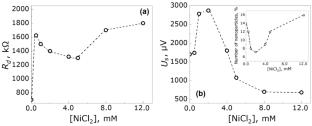
The efficiency of combined donor–acceptor doping of thin lead sulfide films with nickel and iodine ions using the one-pot approach for obtaining photosensitive lead sulfide layers PbS(I, Ni) was shown. Chemical bath deposition of the lead sulfide films from an ammonia-citrate reaction mixture with a combined additive of NH4I and NiCl2 was carried. The conditions for the films deposition were preliminarily determined by analyzing ionic equilibria in an ammonia-citrate reaction mixture. Composition, morphology and structure of the synthesized layers were studied using scanning electron microscopy, energy-dispersive elemental analysis and X-ray diffraction. Non-monotonic changes of the content of the main elements Pb, S, I, and Ni in the lead sulfide films, lattice parameter, crystallographic orientation of grains, microstresses and coherent scattering regions, as well as band gap depending on the concentration of NiCl2 in the reaction bath with extreme values near 1–2 mM NiCl2 were revealed. The analysis of Raman and Fourier-transform infrared transmission spectra showed the formation of diiodine pentoxide I2O5, iodate ion IO3−, and nickel oxide NiO in the PbS(I, Ni) films in addition to the PbI2 phase. A 1.8-fold increase in voltage sensitivity and a 7.5-fold increase in detectivity of the PbS(I, Ni) film deposited in the presence of 0.15 M NH4I and 2 mM NiCl2 compared to the film deposited in the presence of only 0.15 M NH4I were found. A significant increase in voltage sensitivity and detectivity of the PbS(I, Ni) films is caused by a synergistic effect of the doping additives with the formation of photoactive phases of lead iodide and iodine and nickel oxides.
期刊介绍:
The Journal of Materials Science: Materials in Electronics is an established refereed companion to the Journal of Materials Science. It publishes papers on materials and their applications in modern electronics, covering the ground between fundamental science, such as semiconductor physics, and work concerned specifically with applications. It explores the growth and preparation of new materials, as well as their processing, fabrication, bonding and encapsulation, together with the reliability, failure analysis, quality assurance and characterization related to the whole range of applications in electronics. The Journal presents papers in newly developing fields such as low dimensional structures and devices, optoelectronics including III-V compounds, glasses and linear/non-linear crystal materials and lasers, high Tc superconductors, conducting polymers, thick film materials and new contact technologies, as well as the established electronics device and circuit materials.


 求助内容:
求助内容: 应助结果提醒方式:


