Intisar A. Naseef, Layla A. Wali, Alwan M. Alwan, Mehdi Q. Zayer
{"title":"多孔、预蚀刻和活化硅表面作为SERS传感器有效性的比较研究","authors":"Intisar A. Naseef, Layla A. Wali, Alwan M. Alwan, Mehdi Q. Zayer","doi":"10.1007/s11468-024-02590-0","DOIUrl":null,"url":null,"abstract":"<div><p>New, easy, and less complicated formation pathways of silicon (Si) surface structures and the well-known photo-electrochemical etching process have been presented and investigated successfully. These pathways included the pre-etching and the activation processes. Significant arrays of silicon surface structures and topographies were achieved as porous, pre-etched, and activated surfaces. These structures have been used as substrates for the palladium nanoparticle (PdNP) deposition process. The investigations of the samples include structural and optical examinations. For porous silicon samples, the obtained field emission scanning electron microscope (FESEM) results showed large microscale pores with 0.387 µm average diameter and small nanoscale pores formed inside them with 21.61 nm average diameter. Such a porous nature affords a larger surface area within a compact volume, for the pre-etched silicon samples nanoscale pores were exhibited with an average pore diameter of 62.62 nm distributed evenly on the surface. Lastly, for the activated silicon samples; the once-smooth silicon surface displays a texture with a noticeable uneven appearance, microscopic irregularities, grooves, and scarped areas with an average roughness of 6.6 µm and root mean square of 12.853 µm. It is shown that surface-enhanced Raman spectroscopy of these structure-coated PdNP substrates could successfully detect nitrate at low concentrations. In particular, the pre-etched Si structure exhibited the highest enhancement factor of (1.79 × 10<sup>11</sup>).</p></div>","PeriodicalId":736,"journal":{"name":"Plasmonics","volume":"20 9","pages":"7239 - 7257"},"PeriodicalIF":4.3000,"publicationDate":"2025-01-23","publicationTypes":"Journal Article","fieldsOfStudy":null,"isOpenAccess":false,"openAccessPdf":"","citationCount":"0","resultStr":"{\"title\":\"A Comparative Study of the Effectiveness of Porous, Pre-etched, and Activated Silicon Surfaces as SERS Sensors\",\"authors\":\"Intisar A. Naseef, Layla A. Wali, Alwan M. Alwan, Mehdi Q. Zayer\",\"doi\":\"10.1007/s11468-024-02590-0\",\"DOIUrl\":null,\"url\":null,\"abstract\":\"<div><p>New, easy, and less complicated formation pathways of silicon (Si) surface structures and the well-known photo-electrochemical etching process have been presented and investigated successfully. These pathways included the pre-etching and the activation processes. Significant arrays of silicon surface structures and topographies were achieved as porous, pre-etched, and activated surfaces. These structures have been used as substrates for the palladium nanoparticle (PdNP) deposition process. The investigations of the samples include structural and optical examinations. For porous silicon samples, the obtained field emission scanning electron microscope (FESEM) results showed large microscale pores with 0.387 µm average diameter and small nanoscale pores formed inside them with 21.61 nm average diameter. Such a porous nature affords a larger surface area within a compact volume, for the pre-etched silicon samples nanoscale pores were exhibited with an average pore diameter of 62.62 nm distributed evenly on the surface. Lastly, for the activated silicon samples; the once-smooth silicon surface displays a texture with a noticeable uneven appearance, microscopic irregularities, grooves, and scarped areas with an average roughness of 6.6 µm and root mean square of 12.853 µm. It is shown that surface-enhanced Raman spectroscopy of these structure-coated PdNP substrates could successfully detect nitrate at low concentrations. In particular, the pre-etched Si structure exhibited the highest enhancement factor of (1.79 × 10<sup>11</sup>).</p></div>\",\"PeriodicalId\":736,\"journal\":{\"name\":\"Plasmonics\",\"volume\":\"20 9\",\"pages\":\"7239 - 7257\"},\"PeriodicalIF\":4.3000,\"publicationDate\":\"2025-01-23\",\"publicationTypes\":\"Journal Article\",\"fieldsOfStudy\":null,\"isOpenAccess\":false,\"openAccessPdf\":\"\",\"citationCount\":\"0\",\"resultStr\":null,\"platform\":\"Semanticscholar\",\"paperid\":null,\"PeriodicalName\":\"Plasmonics\",\"FirstCategoryId\":\"101\",\"ListUrlMain\":\"https://link.springer.com/article/10.1007/s11468-024-02590-0\",\"RegionNum\":4,\"RegionCategory\":\"物理与天体物理\",\"ArticlePicture\":[],\"TitleCN\":null,\"AbstractTextCN\":null,\"PMCID\":null,\"EPubDate\":\"\",\"PubModel\":\"\",\"JCR\":\"Q2\",\"JCRName\":\"CHEMISTRY, PHYSICAL\",\"Score\":null,\"Total\":0}","platform":"Semanticscholar","paperid":null,"PeriodicalName":"Plasmonics","FirstCategoryId":"101","ListUrlMain":"https://link.springer.com/article/10.1007/s11468-024-02590-0","RegionNum":4,"RegionCategory":"物理与天体物理","ArticlePicture":[],"TitleCN":null,"AbstractTextCN":null,"PMCID":null,"EPubDate":"","PubModel":"","JCR":"Q2","JCRName":"CHEMISTRY, PHYSICAL","Score":null,"Total":0}
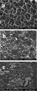
A Comparative Study of the Effectiveness of Porous, Pre-etched, and Activated Silicon Surfaces as SERS Sensors
New, easy, and less complicated formation pathways of silicon (Si) surface structures and the well-known photo-electrochemical etching process have been presented and investigated successfully. These pathways included the pre-etching and the activation processes. Significant arrays of silicon surface structures and topographies were achieved as porous, pre-etched, and activated surfaces. These structures have been used as substrates for the palladium nanoparticle (PdNP) deposition process. The investigations of the samples include structural and optical examinations. For porous silicon samples, the obtained field emission scanning electron microscope (FESEM) results showed large microscale pores with 0.387 µm average diameter and small nanoscale pores formed inside them with 21.61 nm average diameter. Such a porous nature affords a larger surface area within a compact volume, for the pre-etched silicon samples nanoscale pores were exhibited with an average pore diameter of 62.62 nm distributed evenly on the surface. Lastly, for the activated silicon samples; the once-smooth silicon surface displays a texture with a noticeable uneven appearance, microscopic irregularities, grooves, and scarped areas with an average roughness of 6.6 µm and root mean square of 12.853 µm. It is shown that surface-enhanced Raman spectroscopy of these structure-coated PdNP substrates could successfully detect nitrate at low concentrations. In particular, the pre-etched Si structure exhibited the highest enhancement factor of (1.79 × 10¹¹).
期刊介绍:
Plasmonics is an international forum for the publication of peer-reviewed leading-edge original articles that both advance and report our knowledge base and practice of the interactions of free-metal electrons, Plasmons.
Topics covered include notable advances in the theory, Physics, and applications of surface plasmons in metals, to the rapidly emerging areas of nanotechnology, biophotonics, sensing, biochemistry and medicine. Topics, including the theory, synthesis and optical properties of noble metal nanostructures, patterned surfaces or materials, continuous or grated surfaces, devices, or wires for their multifarious applications are particularly welcome. Typical applications might include but are not limited to, surface enhanced spectroscopic properties, such as Raman scattering or fluorescence, as well developments in techniques such as surface plasmon resonance and near-field scanning optical microscopy.


 求助内容:
求助内容: 应助结果提醒方式:


