K. Rodriguez-Rosales, Jorge Cruz-Gómez, José Santos-Cruz, M. Meléndez-Lira, A. Guillén-Cervantes, G. Contreras-Puente, Francisco Javier de Moure-Flores
{"title":"PVD沉积CuI薄膜厚度对CdS/CdTe太阳能电池性能的影响","authors":"K. Rodriguez-Rosales, Jorge Cruz-Gómez, José Santos-Cruz, M. Meléndez-Lira, A. Guillén-Cervantes, G. Contreras-Puente, Francisco Javier de Moure-Flores","doi":"10.1007/s10854-025-15787-8","DOIUrl":null,"url":null,"abstract":"<div><p>Copper iodide (CuI) is a p-type semiconductor with promising applications in optoelectronic devices, particularly as a buffer layer in CdS/CdTe heterojunction solar cells. Its implementation can effectively reduce charge transport losses from the CdTe absorber layer to the back electrode, typically composed of Cu/Au. In this study, CuI thin films with thicknesses ranging from 2 to 100 nm were deposited via physical vapor deposition (PVD). The optoelectronic, morphological, and structural properties of these films were systematically analyzed both with and without post-deposition thermal treatment. Based on these analyses, each CuI film, 6, 20, 40, 60, and 100 nm thick (as grown), was integrated as a buffer layer in four CdS/CdTe solar cells. The obtained data had a low standard deviation, showing low dispersion and good reproducibility. Among these, the 20 nm CuI buffer layer exhibited the best performance, surpassing the reference solar cell without a buffer layer. The optimized devices exhibited a 44% increase in short-circuit current density and a 29% improvement in power conversion efficiency on average, despite a 3% decrease in open-circuit voltage compared to the control cell. Since copper diffusion is the primary issue that reduces the lifetime of CdS/CdTe solar cells, it is expected that the lifetime will increase as the metallic copper back contact is replaced with CuI. These findings highlight the potential of CuI as an effective buffer layer to improve the performance of CdS/CdTe solar cells.</p></div>","PeriodicalId":646,"journal":{"name":"Journal of Materials Science: Materials in Electronics","volume":"36 26","pages":""},"PeriodicalIF":2.8000,"publicationDate":"2025-09-18","publicationTypes":"Journal Article","fieldsOfStudy":null,"isOpenAccess":false,"openAccessPdf":"","citationCount":"0","resultStr":"{\"title\":\"Effect of CuI film thickness deposited via PVD on the performance of CdS/CdTe solar cells\",\"authors\":\"K. Rodriguez-Rosales, Jorge Cruz-Gómez, José Santos-Cruz, M. Meléndez-Lira, A. Guillén-Cervantes, G. Contreras-Puente, Francisco Javier de Moure-Flores\",\"doi\":\"10.1007/s10854-025-15787-8\",\"DOIUrl\":null,\"url\":null,\"abstract\":\"<div><p>Copper iodide (CuI) is a p-type semiconductor with promising applications in optoelectronic devices, particularly as a buffer layer in CdS/CdTe heterojunction solar cells. Its implementation can effectively reduce charge transport losses from the CdTe absorber layer to the back electrode, typically composed of Cu/Au. In this study, CuI thin films with thicknesses ranging from 2 to 100 nm were deposited via physical vapor deposition (PVD). The optoelectronic, morphological, and structural properties of these films were systematically analyzed both with and without post-deposition thermal treatment. Based on these analyses, each CuI film, 6, 20, 40, 60, and 100 nm thick (as grown), was integrated as a buffer layer in four CdS/CdTe solar cells. The obtained data had a low standard deviation, showing low dispersion and good reproducibility. Among these, the 20 nm CuI buffer layer exhibited the best performance, surpassing the reference solar cell without a buffer layer. The optimized devices exhibited a 44% increase in short-circuit current density and a 29% improvement in power conversion efficiency on average, despite a 3% decrease in open-circuit voltage compared to the control cell. Since copper diffusion is the primary issue that reduces the lifetime of CdS/CdTe solar cells, it is expected that the lifetime will increase as the metallic copper back contact is replaced with CuI. These findings highlight the potential of CuI as an effective buffer layer to improve the performance of CdS/CdTe solar cells.</p></div>\",\"PeriodicalId\":646,\"journal\":{\"name\":\"Journal of Materials Science: Materials in Electronics\",\"volume\":\"36 26\",\"pages\":\"\"},\"PeriodicalIF\":2.8000,\"publicationDate\":\"2025-09-18\",\"publicationTypes\":\"Journal Article\",\"fieldsOfStudy\":null,\"isOpenAccess\":false,\"openAccessPdf\":\"\",\"citationCount\":\"0\",\"resultStr\":null,\"platform\":\"Semanticscholar\",\"paperid\":null,\"PeriodicalName\":\"Journal of Materials Science: Materials in Electronics\",\"FirstCategoryId\":\"5\",\"ListUrlMain\":\"https://link.springer.com/article/10.1007/s10854-025-15787-8\",\"RegionNum\":4,\"RegionCategory\":\"工程技术\",\"ArticlePicture\":[],\"TitleCN\":null,\"AbstractTextCN\":null,\"PMCID\":null,\"EPubDate\":\"\",\"PubModel\":\"\",\"JCR\":\"Q2\",\"JCRName\":\"ENGINEERING, ELECTRICAL & ELECTRONIC\",\"Score\":null,\"Total\":0}","platform":"Semanticscholar","paperid":null,"PeriodicalName":"Journal of Materials Science: Materials in Electronics","FirstCategoryId":"5","ListUrlMain":"https://link.springer.com/article/10.1007/s10854-025-15787-8","RegionNum":4,"RegionCategory":"工程技术","ArticlePicture":[],"TitleCN":null,"AbstractTextCN":null,"PMCID":null,"EPubDate":"","PubModel":"","JCR":"Q2","JCRName":"ENGINEERING, ELECTRICAL & ELECTRONIC","Score":null,"Total":0}
Effect of CuI film thickness deposited via PVD on the performance of CdS/CdTe solar cells
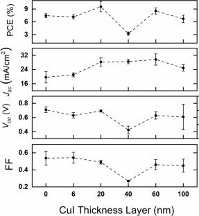
Copper iodide (CuI) is a p-type semiconductor with promising applications in optoelectronic devices, particularly as a buffer layer in CdS/CdTe heterojunction solar cells. Its implementation can effectively reduce charge transport losses from the CdTe absorber layer to the back electrode, typically composed of Cu/Au. In this study, CuI thin films with thicknesses ranging from 2 to 100 nm were deposited via physical vapor deposition (PVD). The optoelectronic, morphological, and structural properties of these films were systematically analyzed both with and without post-deposition thermal treatment. Based on these analyses, each CuI film, 6, 20, 40, 60, and 100 nm thick (as grown), was integrated as a buffer layer in four CdS/CdTe solar cells. The obtained data had a low standard deviation, showing low dispersion and good reproducibility. Among these, the 20 nm CuI buffer layer exhibited the best performance, surpassing the reference solar cell without a buffer layer. The optimized devices exhibited a 44% increase in short-circuit current density and a 29% improvement in power conversion efficiency on average, despite a 3% decrease in open-circuit voltage compared to the control cell. Since copper diffusion is the primary issue that reduces the lifetime of CdS/CdTe solar cells, it is expected that the lifetime will increase as the metallic copper back contact is replaced with CuI. These findings highlight the potential of CuI as an effective buffer layer to improve the performance of CdS/CdTe solar cells.
期刊介绍:
The Journal of Materials Science: Materials in Electronics is an established refereed companion to the Journal of Materials Science. It publishes papers on materials and their applications in modern electronics, covering the ground between fundamental science, such as semiconductor physics, and work concerned specifically with applications. It explores the growth and preparation of new materials, as well as their processing, fabrication, bonding and encapsulation, together with the reliability, failure analysis, quality assurance and characterization related to the whole range of applications in electronics. The Journal presents papers in newly developing fields such as low dimensional structures and devices, optoelectronics including III-V compounds, glasses and linear/non-linear crystal materials and lasers, high Tc superconductors, conducting polymers, thick film materials and new contact technologies, as well as the established electronics device and circuit materials.

 求助内容:
求助内容: 应助结果提醒方式:


