Yunxuan Zhu, Sai C. Yelishala, Shusen Liao, Jackson Shropshire, Douglas Natelson, Longji Cui
{"title":"片上单晶等离子体光电子技术,用于高效热载流子收集和光电压检测","authors":"Yunxuan Zhu, Sai C. Yelishala, Shusen Liao, Jackson Shropshire, Douglas Natelson, Longji Cui","doi":"10.1038/s41377-025-02030-6","DOIUrl":null,"url":null,"abstract":"<p>Large-area chemically synthesized single-crystal metals with nanometer-scale thickness have emerged as promising materials for on-chip nanophotonic applications, owing to their superior plasmonic properties compared to nanofabricated polycrystalline counterparts. While much recent attention has focused on their optical properties, the combined optimal electrical and optical characteristics, which hold great potential for high-performance optoelectronic functionalities, remain largely unexplored. Here, we present a single-crystal plasmonic optoelectronic platform based on nanowires fabricated from synthesized gold flakes and demonstrate its capabilities for highly enhanced hot carrier collection, electroluminescence, and photovoltage detection. Notably, single-crystal gold nanogap devices exhibit an order of magnitude higher open-circuit photovoltage compared to polycrystalline devices, representing one of the highest reported photovoltage sensing performances in terms of on-chip device density and responsivity per area. Our analysis revealed that this enhancement is attributed mostly to the suppression of electron-phonon scattering and improved hot carrier tunneling efficiency in single-crystal devices. These results highlight the potential of large-scale single-crystal nanostructures for both fundamental studies of nanoscale hot carrier transport and scalable electrically driven nanophotonic applications.</p>","PeriodicalId":18069,"journal":{"name":"Light-Science & Applications","volume":"1 1","pages":""},"PeriodicalIF":23.4000,"publicationDate":"2025-09-16","publicationTypes":"Journal Article","fieldsOfStudy":null,"isOpenAccess":false,"openAccessPdf":"","citationCount":"0","resultStr":"{\"title\":\"On-chip single-crystal plasmonic optoelectronics for efficient hot carrier collection and photovoltage detection\",\"authors\":\"Yunxuan Zhu, Sai C. Yelishala, Shusen Liao, Jackson Shropshire, Douglas Natelson, Longji Cui\",\"doi\":\"10.1038/s41377-025-02030-6\",\"DOIUrl\":null,\"url\":null,\"abstract\":\"<p>Large-area chemically synthesized single-crystal metals with nanometer-scale thickness have emerged as promising materials for on-chip nanophotonic applications, owing to their superior plasmonic properties compared to nanofabricated polycrystalline counterparts. While much recent attention has focused on their optical properties, the combined optimal electrical and optical characteristics, which hold great potential for high-performance optoelectronic functionalities, remain largely unexplored. Here, we present a single-crystal plasmonic optoelectronic platform based on nanowires fabricated from synthesized gold flakes and demonstrate its capabilities for highly enhanced hot carrier collection, electroluminescence, and photovoltage detection. Notably, single-crystal gold nanogap devices exhibit an order of magnitude higher open-circuit photovoltage compared to polycrystalline devices, representing one of the highest reported photovoltage sensing performances in terms of on-chip device density and responsivity per area. Our analysis revealed that this enhancement is attributed mostly to the suppression of electron-phonon scattering and improved hot carrier tunneling efficiency in single-crystal devices. These results highlight the potential of large-scale single-crystal nanostructures for both fundamental studies of nanoscale hot carrier transport and scalable electrically driven nanophotonic applications.</p>\",\"PeriodicalId\":18069,\"journal\":{\"name\":\"Light-Science & Applications\",\"volume\":\"1 1\",\"pages\":\"\"},\"PeriodicalIF\":23.4000,\"publicationDate\":\"2025-09-16\",\"publicationTypes\":\"Journal Article\",\"fieldsOfStudy\":null,\"isOpenAccess\":false,\"openAccessPdf\":\"\",\"citationCount\":\"0\",\"resultStr\":null,\"platform\":\"Semanticscholar\",\"paperid\":null,\"PeriodicalName\":\"Light-Science & Applications\",\"FirstCategoryId\":\"1089\",\"ListUrlMain\":\"https://doi.org/10.1038/s41377-025-02030-6\",\"RegionNum\":0,\"RegionCategory\":null,\"ArticlePicture\":[],\"TitleCN\":null,\"AbstractTextCN\":null,\"PMCID\":null,\"EPubDate\":\"\",\"PubModel\":\"\",\"JCR\":\"Q1\",\"JCRName\":\"OPTICS\",\"Score\":null,\"Total\":0}","platform":"Semanticscholar","paperid":null,"PeriodicalName":"Light-Science & Applications","FirstCategoryId":"1089","ListUrlMain":"https://doi.org/10.1038/s41377-025-02030-6","RegionNum":0,"RegionCategory":null,"ArticlePicture":[],"TitleCN":null,"AbstractTextCN":null,"PMCID":null,"EPubDate":"","PubModel":"","JCR":"Q1","JCRName":"OPTICS","Score":null,"Total":0}
On-chip single-crystal plasmonic optoelectronics for efficient hot carrier collection and photovoltage detection
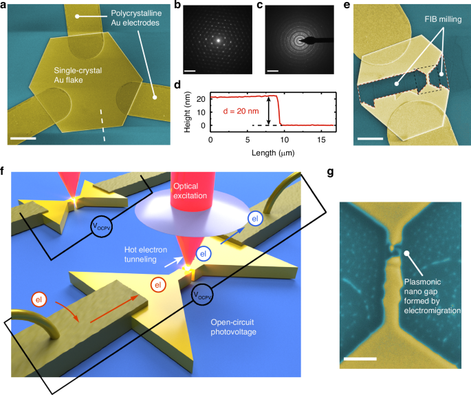
Large-area chemically synthesized single-crystal metals with nanometer-scale thickness have emerged as promising materials for on-chip nanophotonic applications, owing to their superior plasmonic properties compared to nanofabricated polycrystalline counterparts. While much recent attention has focused on their optical properties, the combined optimal electrical and optical characteristics, which hold great potential for high-performance optoelectronic functionalities, remain largely unexplored. Here, we present a single-crystal plasmonic optoelectronic platform based on nanowires fabricated from synthesized gold flakes and demonstrate its capabilities for highly enhanced hot carrier collection, electroluminescence, and photovoltage detection. Notably, single-crystal gold nanogap devices exhibit an order of magnitude higher open-circuit photovoltage compared to polycrystalline devices, representing one of the highest reported photovoltage sensing performances in terms of on-chip device density and responsivity per area. Our analysis revealed that this enhancement is attributed mostly to the suppression of electron-phonon scattering and improved hot carrier tunneling efficiency in single-crystal devices. These results highlight the potential of large-scale single-crystal nanostructures for both fundamental studies of nanoscale hot carrier transport and scalable electrically driven nanophotonic applications.
 求助内容:
求助内容: 应助结果提醒方式:


