{"title":"多晶热电材料晶界限制输运的统一迁移率模型","authors":"Gbadebo Taofeek Yusuf , Sukhwinder Singh , Alexandros Askounis , Zlatka Stoeva , Fideline Tchuenbou-Magaia","doi":"10.1016/j.mtla.2025.102550","DOIUrl":null,"url":null,"abstract":"<div><div>Grain-boundary-limited charge transport is a fundamental bottleneck in polycrystalline thermoelectric materials, where reduced carrier mobility degrades electrical conductivity and suppresses power factors. This degradation arises from the interplay of scattering mechanisms: grain-boundary barriers dominate at low temperatures; thermionic activation enables partial barrier crossing at intermediate temperatures; and phonon scattering limits the mean free path at high temperatures. Hence, there remains a need for a physically transparent framework to quantitatively extract these microstructural parameters. In this study, a semi-empirical mobility model that explicitly integrates these grain-boundary mechanisms was developed and validated, expressed as: <span><math><mrow><msub><mi>μ</mi><mrow><mi>e</mi><mi>f</mi><mi>f</mi></mrow></msub><mrow><mo>(</mo><mi>T</mi><mo>)</mo></mrow><mo>=</mo><msub><mi>μ</mi><mi>w</mi></msub><mtext>exp</mtext><mrow><mo>(</mo><mrow><mo>−</mo><mfrac><msub><mstyle><mi>Φ</mi></mstyle><mrow><mi>G</mi><mi>B</mi></mrow></msub><mrow><msub><mi>k</mi><mi>B</mi></msub><mi>T</mi></mrow></mfrac></mrow><mo>)</mo></mrow><mfrac><mrow><mi>l</mi><mo>(</mo><mi>T</mi><mo>)</mo></mrow><mrow><mi>l</mi><mrow><mo>(</mo><mi>T</mi><mo>)</mo></mrow><mo>+</mo><msub><mi>w</mi><mrow><mi>G</mi><mi>B</mi></mrow></msub></mrow></mfrac></mrow></math></span> where <span><math><msub><mi>μ</mi><mi>w</mi></msub></math></span> is the weighted mobility, <span><math><msub><mstyle><mi>Φ</mi></mstyle><mrow><mi>G</mi><mi>B</mi></mrow></msub></math></span> is the grain‑boundary barrier height, <span><math><msub><mi>k</mi><mi>B</mi></msub></math></span> is Boltzmann’s constant, <span><math><mi>T</mi></math></span> is temperature, <span><math><mrow><mi>l</mi><mo>(</mo><mi>T</mi><mo>)</mo></mrow></math></span> is the bulk mean free path and <span><math><msub><mi>w</mi><mrow><mi>G</mi><mi>B</mi></mrow></msub></math></span> is the boundary width. This model was validated for oxide semiconductor, intermetallic, chalcogenide and heuslers polycrystalline materials, achieving excellent agreement with experimental data (<span><math><msup><mrow><mi>R</mi></mrow><mn>2</mn></msup></math></span>= 0.97–0.99) and yielding physically consistent parameters: <span><math><msub><mstyle><mi>Φ</mi></mstyle><mrow><mi>G</mi><mi>B</mi></mrow></msub></math></span> ≈ 0–0.056 eV and <span><math><msub><mi>l</mi><mn>300</mn></msub></math></span> ≈ 6–368 nm. A case study for Ta doped ZnO thermoelectric material shows that barrier passivation (reduction of <span><math><msub><mstyle><mi>Φ</mi></mstyle><mrow><mi>G</mi><mi>B</mi></mrow></msub></math></span> from 0.056 eV to 0.03 eV) combined with modest grain-interior improvement (<span><math><msub><mi>l</mi><mn>300</mn></msub></math></span>→60 nm) can significantly enhance carrier mobility across the entire temperature range. The analysis predicts that, at ∼1000 K, grain engineering could nearly double mobility and electrical conductivity. Consequently, tailoring microstructural features enable a power factor approximately of 7.64x<span><math><msup><mrow><mn>10</mn></mrow><mrow><mo>−</mo><mn>4</mn></mrow></msup></math></span>W<span><math><mrow><msup><mrow><mi>m</mi></mrow><mrow><mo>−</mo><mn>1</mn></mrow></msup><msup><mrow><mi>K</mi></mrow><mrow><mo>−</mo><mn>2</mn></mrow></msup></mrow></math></span> at 1000 K, compared with the reported value of 4x<span><math><msup><mrow><mn>10</mn></mrow><mrow><mo>−</mo><mn>4</mn></mrow></msup></math></span>W<span><math><mrow><msup><mrow><mi>m</mi></mrow><mrow><mo>−</mo><mn>1</mn></mrow></msup><msup><mrow><mi>K</mi></mrow><mrow><mo>−</mo><mn>2</mn></mrow></msup></mrow></math></span>. This framework provides concrete, process-addressable targets for grain-boundary engineering and mobility-driven performance gains.</div></div>","PeriodicalId":47623,"journal":{"name":"Materialia","volume":"44 ","pages":"Article 102550"},"PeriodicalIF":2.9000,"publicationDate":"2025-09-08","publicationTypes":"Journal Article","fieldsOfStudy":null,"isOpenAccess":false,"openAccessPdf":"","citationCount":"0","resultStr":"{\"title\":\"Unified mobility model for grain‑boundary‑limited transport in polycrystalline thermoelectric materials\",\"authors\":\"Gbadebo Taofeek Yusuf , Sukhwinder Singh , Alexandros Askounis , Zlatka Stoeva , Fideline Tchuenbou-Magaia\",\"doi\":\"10.1016/j.mtla.2025.102550\",\"DOIUrl\":null,\"url\":null,\"abstract\":\"<div><div>Grain-boundary-limited charge transport is a fundamental bottleneck in polycrystalline thermoelectric materials, where reduced carrier mobility degrades electrical conductivity and suppresses power factors. This degradation arises from the interplay of scattering mechanisms: grain-boundary barriers dominate at low temperatures; thermionic activation enables partial barrier crossing at intermediate temperatures; and phonon scattering limits the mean free path at high temperatures. Hence, there remains a need for a physically transparent framework to quantitatively extract these microstructural parameters. In this study, a semi-empirical mobility model that explicitly integrates these grain-boundary mechanisms was developed and validated, expressed as: <span><math><mrow><msub><mi>μ</mi><mrow><mi>e</mi><mi>f</mi><mi>f</mi></mrow></msub><mrow><mo>(</mo><mi>T</mi><mo>)</mo></mrow><mo>=</mo><msub><mi>μ</mi><mi>w</mi></msub><mtext>exp</mtext><mrow><mo>(</mo><mrow><mo>−</mo><mfrac><msub><mstyle><mi>Φ</mi></mstyle><mrow><mi>G</mi><mi>B</mi></mrow></msub><mrow><msub><mi>k</mi><mi>B</mi></msub><mi>T</mi></mrow></mfrac></mrow><mo>)</mo></mrow><mfrac><mrow><mi>l</mi><mo>(</mo><mi>T</mi><mo>)</mo></mrow><mrow><mi>l</mi><mrow><mo>(</mo><mi>T</mi><mo>)</mo></mrow><mo>+</mo><msub><mi>w</mi><mrow><mi>G</mi><mi>B</mi></mrow></msub></mrow></mfrac></mrow></math></span> where <span><math><msub><mi>μ</mi><mi>w</mi></msub></math></span> is the weighted mobility, <span><math><msub><mstyle><mi>Φ</mi></mstyle><mrow><mi>G</mi><mi>B</mi></mrow></msub></math></span> is the grain‑boundary barrier height, <span><math><msub><mi>k</mi><mi>B</mi></msub></math></span> is Boltzmann’s constant, <span><math><mi>T</mi></math></span> is temperature, <span><math><mrow><mi>l</mi><mo>(</mo><mi>T</mi><mo>)</mo></mrow></math></span> is the bulk mean free path and <span><math><msub><mi>w</mi><mrow><mi>G</mi><mi>B</mi></mrow></msub></math></span> is the boundary width. This model was validated for oxide semiconductor, intermetallic, chalcogenide and heuslers polycrystalline materials, achieving excellent agreement with experimental data (<span><math><msup><mrow><mi>R</mi></mrow><mn>2</mn></msup></math></span>= 0.97–0.99) and yielding physically consistent parameters: <span><math><msub><mstyle><mi>Φ</mi></mstyle><mrow><mi>G</mi><mi>B</mi></mrow></msub></math></span> ≈ 0–0.056 eV and <span><math><msub><mi>l</mi><mn>300</mn></msub></math></span> ≈ 6–368 nm. A case study for Ta doped ZnO thermoelectric material shows that barrier passivation (reduction of <span><math><msub><mstyle><mi>Φ</mi></mstyle><mrow><mi>G</mi><mi>B</mi></mrow></msub></math></span> from 0.056 eV to 0.03 eV) combined with modest grain-interior improvement (<span><math><msub><mi>l</mi><mn>300</mn></msub></math></span>→60 nm) can significantly enhance carrier mobility across the entire temperature range. The analysis predicts that, at ∼1000 K, grain engineering could nearly double mobility and electrical conductivity. Consequently, tailoring microstructural features enable a power factor approximately of 7.64x<span><math><msup><mrow><mn>10</mn></mrow><mrow><mo>−</mo><mn>4</mn></mrow></msup></math></span>W<span><math><mrow><msup><mrow><mi>m</mi></mrow><mrow><mo>−</mo><mn>1</mn></mrow></msup><msup><mrow><mi>K</mi></mrow><mrow><mo>−</mo><mn>2</mn></mrow></msup></mrow></math></span> at 1000 K, compared with the reported value of 4x<span><math><msup><mrow><mn>10</mn></mrow><mrow><mo>−</mo><mn>4</mn></mrow></msup></math></span>W<span><math><mrow><msup><mrow><mi>m</mi></mrow><mrow><mo>−</mo><mn>1</mn></mrow></msup><msup><mrow><mi>K</mi></mrow><mrow><mo>−</mo><mn>2</mn></mrow></msup></mrow></math></span>. This framework provides concrete, process-addressable targets for grain-boundary engineering and mobility-driven performance gains.</div></div>\",\"PeriodicalId\":47623,\"journal\":{\"name\":\"Materialia\",\"volume\":\"44 \",\"pages\":\"Article 102550\"},\"PeriodicalIF\":2.9000,\"publicationDate\":\"2025-09-08\",\"publicationTypes\":\"Journal Article\",\"fieldsOfStudy\":null,\"isOpenAccess\":false,\"openAccessPdf\":\"\",\"citationCount\":\"0\",\"resultStr\":null,\"platform\":\"Semanticscholar\",\"paperid\":null,\"PeriodicalName\":\"Materialia\",\"FirstCategoryId\":\"1085\",\"ListUrlMain\":\"https://www.sciencedirect.com/science/article/pii/S2589152925002182\",\"RegionNum\":0,\"RegionCategory\":null,\"ArticlePicture\":[],\"TitleCN\":null,\"AbstractTextCN\":null,\"PMCID\":null,\"EPubDate\":\"\",\"PubModel\":\"\",\"JCR\":\"Q2\",\"JCRName\":\"MATERIALS SCIENCE, MULTIDISCIPLINARY\",\"Score\":null,\"Total\":0}","platform":"Semanticscholar","paperid":null,"PeriodicalName":"Materialia","FirstCategoryId":"1085","ListUrlMain":"https://www.sciencedirect.com/science/article/pii/S2589152925002182","RegionNum":0,"RegionCategory":null,"ArticlePicture":[],"TitleCN":null,"AbstractTextCN":null,"PMCID":null,"EPubDate":"","PubModel":"","JCR":"Q2","JCRName":"MATERIALS SCIENCE, MULTIDISCIPLINARY","Score":null,"Total":0}
Unified mobility model for grain‑boundary‑limited transport in polycrystalline thermoelectric materials
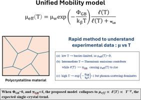
Grain-boundary-limited charge transport is a fundamental bottleneck in polycrystalline thermoelectric materials, where reduced carrier mobility degrades electrical conductivity and suppresses power factors. This degradation arises from the interplay of scattering mechanisms: grain-boundary barriers dominate at low temperatures; thermionic activation enables partial barrier crossing at intermediate temperatures; and phonon scattering limits the mean free path at high temperatures. Hence, there remains a need for a physically transparent framework to quantitatively extract these microstructural parameters. In this study, a semi-empirical mobility model that explicitly integrates these grain-boundary mechanisms was developed and validated, expressed as: where is the weighted mobility, is the grain‑boundary barrier height, is Boltzmann’s constant, is temperature, is the bulk mean free path and is the boundary width. This model was validated for oxide semiconductor, intermetallic, chalcogenide and heuslers polycrystalline materials, achieving excellent agreement with experimental data (= 0.97–0.99) and yielding physically consistent parameters: ≈ 0–0.056 eV and ≈ 6–368 nm. A case study for Ta doped ZnO thermoelectric material shows that barrier passivation (reduction of from 0.056 eV to 0.03 eV) combined with modest grain-interior improvement (→60 nm) can significantly enhance carrier mobility across the entire temperature range. The analysis predicts that, at ∼1000 K, grain engineering could nearly double mobility and electrical conductivity. Consequently, tailoring microstructural features enable a power factor approximately of 7.64xW at 1000 K, compared with the reported value of 4xW. This framework provides concrete, process-addressable targets for grain-boundary engineering and mobility-driven performance gains.
期刊介绍:
Materialia is a multidisciplinary journal of materials science and engineering that publishes original peer-reviewed research articles. Articles in Materialia advance the understanding of the relationship between processing, structure, property, and function of materials.
Materialia publishes full-length research articles, review articles, and letters (short communications). In addition to receiving direct submissions, Materialia also accepts transfers from Acta Materialia, Inc. partner journals. Materialia offers authors the choice to publish on an open access model (with author fee), or on a subscription model (with no author fee).
 求助内容:
求助内容: 应助结果提醒方式:


