芯片尺寸对边缘端接SiC mosfet动态特性的影响

Y. Kim, H. Kang
{"title":"芯片尺寸对边缘端接SiC mosfet动态特性的影响","authors":"Y. Kim,&nbsp;H. Kang","doi":"10.1016/j.pedc.2025.100110","DOIUrl":null,"url":null,"abstract":"<div><div>This study investigates the impact of the active-to-termination area ratio on the dynamic behavior of SiC MOSFETs. As the chip size decreases, the turn-on speed increases due to the reduced input capacitance. However, during the turn-off transient, a <em>dV/dt</em> reversal effect is observed, in which the switching speed decreases despite the overall reduction in parasitic capacitance. This effect arises because, in smaller devices, the edge termination region becomes relatively larger compared to the active region, causing a greater portion of the drain current to flow into the termination region. As a result, the charging of the drain-to-source capacitance in the active region, which dominates the switching transition, slows down. Experimental and mixed-mode simulations confirm that this effect is more pronounced at lower current densities. The study further examines the effect of gate driver capability, showing that a gate driver with high sinking/sourcing capability only maximizes switching frequency. Additionally, thermal resistance and drain-to-source capacitance charging delay limit the maximum switching frequency in smaller devices. These results demonstrate that the active-to-termination area ratio significantly influences the switching characteristics of SiC MOSFETs, particularly in turn-off behavior and frequency limitations.</div></div>","PeriodicalId":74483,"journal":{"name":"Power electronic devices and components","volume":"12 ","pages":"Article 100110"},"PeriodicalIF":0.0000,"publicationDate":"2025-08-28","publicationTypes":"Journal Article","fieldsOfStudy":null,"isOpenAccess":false,"openAccessPdf":"","citationCount":"0","resultStr":"{\"title\":\"Chip size dependent dynamic behavior of SiC MOSFETs with edge termination\",\"authors\":\"Y. Kim,&nbsp;H. Kang\",\"doi\":\"10.1016/j.pedc.2025.100110\",\"DOIUrl\":null,\"url\":null,\"abstract\":\"<div><div>This study investigates the impact of the active-to-termination area ratio on the dynamic behavior of SiC MOSFETs. As the chip size decreases, the turn-on speed increases due to the reduced input capacitance. However, during the turn-off transient, a <em>dV/dt</em> reversal effect is observed, in which the switching speed decreases despite the overall reduction in parasitic capacitance. This effect arises because, in smaller devices, the edge termination region becomes relatively larger compared to the active region, causing a greater portion of the drain current to flow into the termination region. As a result, the charging of the drain-to-source capacitance in the active region, which dominates the switching transition, slows down. Experimental and mixed-mode simulations confirm that this effect is more pronounced at lower current densities. The study further examines the effect of gate driver capability, showing that a gate driver with high sinking/sourcing capability only maximizes switching frequency. Additionally, thermal resistance and drain-to-source capacitance charging delay limit the maximum switching frequency in smaller devices. These results demonstrate that the active-to-termination area ratio significantly influences the switching characteristics of SiC MOSFETs, particularly in turn-off behavior and frequency limitations.</div></div>\",\"PeriodicalId\":74483,\"journal\":{\"name\":\"Power electronic devices and components\",\"volume\":\"12 \",\"pages\":\"Article 100110\"},\"PeriodicalIF\":0.0000,\"publicationDate\":\"2025-08-28\",\"publicationTypes\":\"Journal Article\",\"fieldsOfStudy\":null,\"isOpenAccess\":false,\"openAccessPdf\":\"\",\"citationCount\":\"0\",\"resultStr\":null,\"platform\":\"Semanticscholar\",\"paperid\":null,\"PeriodicalName\":\"Power electronic devices and components\",\"FirstCategoryId\":\"1085\",\"ListUrlMain\":\"https://www.sciencedirect.com/science/article/pii/S2772370425000355\",\"RegionNum\":0,\"RegionCategory\":null,\"ArticlePicture\":[],\"TitleCN\":null,\"AbstractTextCN\":null,\"PMCID\":null,\"EPubDate\":\"\",\"PubModel\":\"\",\"JCR\":\"\",\"JCRName\":\"\",\"Score\":null,\"Total\":0}","platform":"Semanticscholar","paperid":null,"PeriodicalName":"Power electronic devices and components","FirstCategoryId":"1085","ListUrlMain":"https://www.sciencedirect.com/science/article/pii/S2772370425000355","RegionNum":0,"RegionCategory":null,"ArticlePicture":[],"TitleCN":null,"AbstractTextCN":null,"PMCID":null,"EPubDate":"","PubModel":"","JCR":"","JCRName":"","Score":null,"Total":0}
引用次数: 0

摘要

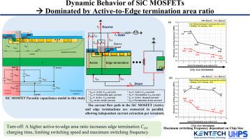
本研究探讨了有源端面积比对SiC mosfet动态特性的影响。随着芯片尺寸的减小,由于输入电容的减小,导通速度增加。然而,在关断瞬态期间,观察到dV/dt反转效应,其中尽管寄生电容总体降低,但开关速度降低。这种效应的产生是因为,在较小的器件中,与有源区相比,边缘终止区变得相对较大,导致更大一部分漏极电流流入终止区。因此,主导开关转换的有源区漏源电容的充电速度减慢。实验和混合模式模拟证实,这种效应在较低的电流密度下更为明显。该研究进一步考察了栅极驱动器能力的影响,表明具有高下沉/源能力的栅极驱动器只能最大化开关频率。此外,热阻和漏源电容充电延迟限制了较小器件的最大开关频率。这些结果表明,有源端面积比显著影响SiC mosfet的开关特性,特别是在关断行为和频率限制方面。
本文章由计算机程序翻译,如有差异,请以英文原文为准。

Chip size dependent dynamic behavior of SiC MOSFETs with edge termination

Chip size dependent dynamic behavior of SiC MOSFETs with edge termination
This study investigates the impact of the active-to-termination area ratio on the dynamic behavior of SiC MOSFETs. As the chip size decreases, the turn-on speed increases due to the reduced input capacitance. However, during the turn-off transient, a dV/dt reversal effect is observed, in which the switching speed decreases despite the overall reduction in parasitic capacitance. This effect arises because, in smaller devices, the edge termination region becomes relatively larger compared to the active region, causing a greater portion of the drain current to flow into the termination region. As a result, the charging of the drain-to-source capacitance in the active region, which dominates the switching transition, slows down. Experimental and mixed-mode simulations confirm that this effect is more pronounced at lower current densities. The study further examines the effect of gate driver capability, showing that a gate driver with high sinking/sourcing capability only maximizes switching frequency. Additionally, thermal resistance and drain-to-source capacitance charging delay limit the maximum switching frequency in smaller devices. These results demonstrate that the active-to-termination area ratio significantly influences the switching characteristics of SiC MOSFETs, particularly in turn-off behavior and frequency limitations.
求助全文
通过发布文献求助,成功后即可免费获取论文全文。 去求助
来源期刊
Power electronic devices and components
Power electronic devices and components Hardware and Architecture, Electrical and Electronic Engineering, Atomic and Molecular Physics, and Optics, Safety, Risk, Reliability and Quality
CiteScore
2.00
自引率
0.00%
发文量
0
审稿时长
80 days
×
引用
GB/T 7714-2015
复制
MLA
复制
APA
复制
导出至
BibTeX EndNote RefMan NoteFirst NoteExpress
×
提示
您的信息不完整,为了账户安全,请先补充。
现在去补充
×
提示
您因"违规操作"
具体请查看互助需知
我知道了
×
提示
确定
请完成安全验证×
copy
已复制链接
快去分享给好友吧!
我知道了
右上角分享
点击右上角分享
0
联系我们:info@booksci.cn Book学术提供免费学术资源搜索服务,方便国内外学者检索中英文文献。致力于提供最便捷和优质的服务体验。 Copyright © 2023 布克学术 All rights reserved.
京ICP备2023020795号-1
ghs 京公网安备 11010802042870号
Book学术文献互助
Book学术文献互助群
群 号:604180095
Book学术官方微信