Jing Yuan , Xiaojuan Chen , Yichuan Zhang , Ying Luo , Binhao Guo , Ke Wei , Yankui Li , Weijun Luo , Weichao Wu , Sen Huang
{"title":"用于毫米波低压应用的低噪声和高功率AlN/GaN miss - hemt","authors":"Jing Yuan , Xiaojuan Chen , Yichuan Zhang , Ying Luo , Binhao Guo , Ke Wei , Yankui Li , Weijun Luo , Weichao Wu , Sen Huang","doi":"10.1016/j.mee.2025.112402","DOIUrl":null,"url":null,"abstract":"<div><div>The SiN<sub>x</sub>/AlN/GaN metal-insulator-semiconductor high electron mobility transistors (MIS-HEMTs) on silicon have been fabricated for low-supply-voltage applications. The devices, featuring a gate length (<em>L</em><sub>g</sub>) of approximately 140 nm, exhibited excellent DC characteristics: a contact resistance (<em>R</em><sub>c</sub>) of 0.24 Ω·mm, a maximum saturated drain current (<em>I</em><sub>dmax</sub>) of 1.86 A/mm at a gate voltage (<em>V</em><sub>gs</sub>) of 2 V, an on-resistance (<em>R</em><sub>on</sub>) of 1.4 Ω·mm, and a peak transconductance (<em>Gm</em><sub>max</sub>) of 466 mS/mm at a drain voltage (<em>V</em><sub>ds</sub>) of 6 V. In RF measurements, the devices achieved ultra-low minimum noise figure (<em>NF</em><sub>min</sub>) of 0.54 (0.66) dB at <em>V</em><sub>ds</sub> of 5 (6) V at 30 GHz, along with a good two-tone linearity, the ratio of output third-order intercept point (<em>OIP</em><sub>3</sub>) to direct current output power (<em>P</em><sub>dc</sub>), denoted as <em>OIP</em><sub>3</sub>/<em>P</em><sub>dc</sub> is 12.4 (9.9) dB at <em>V</em><sub>ds</sub> of 5 (6) V. Pulsed-wave (PW) power measurements indicated the devices have both high output power (<em>P</em><sub>out</sub>) of 1.1 (1.6) W/mm and power-added efficiency (PAE) of 50.2 (49.4 %) at <em>V</em><sub>ds</sub> of 5 (6) V. These results demonstrate the SiN<sub>x</sub>/AlN/GaN MIS-HEMTs on silicon have promising potential in low-supply-voltage mm-wave low-noise and high-power applications.</div></div>","PeriodicalId":18557,"journal":{"name":"Microelectronic Engineering","volume":"302 ","pages":"Article 112402"},"PeriodicalIF":3.1000,"publicationDate":"2025-09-03","publicationTypes":"Journal Article","fieldsOfStudy":null,"isOpenAccess":false,"openAccessPdf":"","citationCount":"0","resultStr":"{\"title\":\"Low-noise and high-power AlN/GaN MIS-HEMTs on silicon for mm-wave low-voltage applications\",\"authors\":\"Jing Yuan , Xiaojuan Chen , Yichuan Zhang , Ying Luo , Binhao Guo , Ke Wei , Yankui Li , Weijun Luo , Weichao Wu , Sen Huang\",\"doi\":\"10.1016/j.mee.2025.112402\",\"DOIUrl\":null,\"url\":null,\"abstract\":\"<div><div>The SiN<sub>x</sub>/AlN/GaN metal-insulator-semiconductor high electron mobility transistors (MIS-HEMTs) on silicon have been fabricated for low-supply-voltage applications. The devices, featuring a gate length (<em>L</em><sub>g</sub>) of approximately 140 nm, exhibited excellent DC characteristics: a contact resistance (<em>R</em><sub>c</sub>) of 0.24 Ω·mm, a maximum saturated drain current (<em>I</em><sub>dmax</sub>) of 1.86 A/mm at a gate voltage (<em>V</em><sub>gs</sub>) of 2 V, an on-resistance (<em>R</em><sub>on</sub>) of 1.4 Ω·mm, and a peak transconductance (<em>Gm</em><sub>max</sub>) of 466 mS/mm at a drain voltage (<em>V</em><sub>ds</sub>) of 6 V. In RF measurements, the devices achieved ultra-low minimum noise figure (<em>NF</em><sub>min</sub>) of 0.54 (0.66) dB at <em>V</em><sub>ds</sub> of 5 (6) V at 30 GHz, along with a good two-tone linearity, the ratio of output third-order intercept point (<em>OIP</em><sub>3</sub>) to direct current output power (<em>P</em><sub>dc</sub>), denoted as <em>OIP</em><sub>3</sub>/<em>P</em><sub>dc</sub> is 12.4 (9.9) dB at <em>V</em><sub>ds</sub> of 5 (6) V. Pulsed-wave (PW) power measurements indicated the devices have both high output power (<em>P</em><sub>out</sub>) of 1.1 (1.6) W/mm and power-added efficiency (PAE) of 50.2 (49.4 %) at <em>V</em><sub>ds</sub> of 5 (6) V. These results demonstrate the SiN<sub>x</sub>/AlN/GaN MIS-HEMTs on silicon have promising potential in low-supply-voltage mm-wave low-noise and high-power applications.</div></div>\",\"PeriodicalId\":18557,\"journal\":{\"name\":\"Microelectronic Engineering\",\"volume\":\"302 \",\"pages\":\"Article 112402\"},\"PeriodicalIF\":3.1000,\"publicationDate\":\"2025-09-03\",\"publicationTypes\":\"Journal Article\",\"fieldsOfStudy\":null,\"isOpenAccess\":false,\"openAccessPdf\":\"\",\"citationCount\":\"0\",\"resultStr\":null,\"platform\":\"Semanticscholar\",\"paperid\":null,\"PeriodicalName\":\"Microelectronic Engineering\",\"FirstCategoryId\":\"5\",\"ListUrlMain\":\"https://www.sciencedirect.com/science/article/pii/S0167931725000917\",\"RegionNum\":4,\"RegionCategory\":\"工程技术\",\"ArticlePicture\":[],\"TitleCN\":null,\"AbstractTextCN\":null,\"PMCID\":null,\"EPubDate\":\"\",\"PubModel\":\"\",\"JCR\":\"Q2\",\"JCRName\":\"ENGINEERING, ELECTRICAL & ELECTRONIC\",\"Score\":null,\"Total\":0}","platform":"Semanticscholar","paperid":null,"PeriodicalName":"Microelectronic Engineering","FirstCategoryId":"5","ListUrlMain":"https://www.sciencedirect.com/science/article/pii/S0167931725000917","RegionNum":4,"RegionCategory":"工程技术","ArticlePicture":[],"TitleCN":null,"AbstractTextCN":null,"PMCID":null,"EPubDate":"","PubModel":"","JCR":"Q2","JCRName":"ENGINEERING, ELECTRICAL & ELECTRONIC","Score":null,"Total":0}
引用次数: 0
摘要
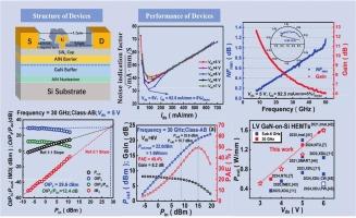
硅基SiNx/AlN/GaN金属-绝缘体-半导体高电子迁移率晶体管(mis - hemt)已制备成功。该器件栅极长度(Lg)约为140 nm,具有优异的直流特性:接触电阻(Rc)为0.24 Ω·mm,栅极电压(Vgs)为2 V时最大饱和漏极电流(Idmax)为1.86 a /mm,导通电阻(Ron)为1.4 Ω·mm,漏极电压(Vds)为6 V时峰值跨导(Gmmax)为466 mS/mm。在射频测量中,该器件在30 GHz的Vds为5 (6)V时实现了0.54 (0.66)dB的超低最小噪声系数(NFmin),同时具有良好的双音线性度,输出三阶截距点(OIP3)与直流输出功率(Pdc)的比值。脉冲波(PW)功率测量表明,该器件在Vds为5 (6)v时具有1.1 (1.6)W/mm的高输出功率(Pout)和50.2(49.4%)的功率附加效率(PAE)。这些结果表明,硅基SiNx/AlN/GaN miss - hemt在低电源电压毫米波低噪声和高功率应用中具有广阔的潜力。
Low-noise and high-power AlN/GaN MIS-HEMTs on silicon for mm-wave low-voltage applications
The SiNx/AlN/GaN metal-insulator-semiconductor high electron mobility transistors (MIS-HEMTs) on silicon have been fabricated for low-supply-voltage applications. The devices, featuring a gate length (Lg) of approximately 140 nm, exhibited excellent DC characteristics: a contact resistance (Rc) of 0.24 Ω·mm, a maximum saturated drain current (Idmax) of 1.86 A/mm at a gate voltage (Vgs) of 2 V, an on-resistance (Ron) of 1.4 Ω·mm, and a peak transconductance (Gmmax) of 466 mS/mm at a drain voltage (Vds) of 6 V. In RF measurements, the devices achieved ultra-low minimum noise figure (NFmin) of 0.54 (0.66) dB at Vds of 5 (6) V at 30 GHz, along with a good two-tone linearity, the ratio of output third-order intercept point (OIP3) to direct current output power (Pdc), denoted as OIP3/Pdc is 12.4 (9.9) dB at Vds of 5 (6) V. Pulsed-wave (PW) power measurements indicated the devices have both high output power (Pout) of 1.1 (1.6) W/mm and power-added efficiency (PAE) of 50.2 (49.4 %) at Vds of 5 (6) V. These results demonstrate the SiNx/AlN/GaN MIS-HEMTs on silicon have promising potential in low-supply-voltage mm-wave low-noise and high-power applications.
期刊介绍:
Microelectronic Engineering is the premier nanoprocessing, and nanotechnology journal focusing on fabrication of electronic, photonic, bioelectronic, electromechanic and fluidic devices and systems, and their applications in the broad areas of electronics, photonics, energy, life sciences, and environment. It covers also the expanding interdisciplinary field of "more than Moore" and "beyond Moore" integrated nanoelectronics / photonics and micro-/nano-/bio-systems. Through its unique mixture of peer-reviewed articles, reviews, accelerated publications, short and Technical notes, and the latest research news on key developments, Microelectronic Engineering provides comprehensive coverage of this exciting, interdisciplinary and dynamic new field for researchers in academia and professionals in industry.