Lan Yang, Dingyuan Niu, Yong Zhang, Xueping Zhao, Xinxin Li, Jun Zhu, Hai Zhang
{"title":"高灵敏度低剂量x射线直接探测β-Ga2O3薄膜的LPCVD和PECVD协同生长","authors":"Lan Yang, Dingyuan Niu, Yong Zhang, Xueping Zhao, Xinxin Li, Jun Zhu, Hai Zhang","doi":"10.3390/nano15171360","DOIUrl":null,"url":null,"abstract":"<p><p>Ultra-wide bandgap β-Ga<sub>2</sub>O<sub>3</sub> is a promising low-cost alternative to conventional direct X-ray detector materials that are limited by fabrication complexity, instability, or slow temporal response. Here, we comparatively investigate β-Ga<sub>2</sub>O<sub>3</sub> thin films grown on c-sapphire by low-pressure chemical vapor deposition (LPCVD) and plasma-enhanced CVD (PECVD), establishing a quantitative linkage between growth kinetics, microstructure, defect landscape, and X-ray detection figures of merit. The LPCVD-grown film (thickness ≈ 0.289 μm) exhibits layered coalesced grains, a narrower rocking curve (FWHM = 1.840°), and deep-level oxygen-vacancy-assisted high photoconductive gain, yielding a high sensitivity of 1.02 × 10<sup>5</sup> μC Gy<sub>air</sub><sup>-1</sup> cm<sup>-2</sup> at 20 V and a thickness-normalized sensitivity of 3.539 × 10<sup>5</sup> μCGy<sub>air</sub><sup>-1</sup> cm<sup>-2</sup> μm<sup>-1</sup>. In contrast, the PECVD-grown film (≈1.57 μm) shows dense columnar growth, higher O/Ga stoichiometric proximity, and shallow-trap dominance, enabling a lower dark current, superior dose detection limit (30.13 vs. 57.07 nGy<sub>air</sub> s<sup>-1</sup>), faster recovery, and monotonic SNR improvement with bias. XPS and dual exponential transient analysis corroborate a deep-trap persistent photoconductivity mechanism in LPCVD versus moderated shallow trapping in PECVD. The resulting high-gain vs. low-noise complementary paradigm clarifies defect-gain trade spaces and provides a route to engineer β-Ga<sub>2</sub>O<sub>3</sub> thin-film X-ray detectors that simultaneously target high sensitivity, low dose limit, and temporal stability through trap and electric field management.</p>","PeriodicalId":18966,"journal":{"name":"Nanomaterials","volume":"15 17","pages":""},"PeriodicalIF":4.3000,"publicationDate":"2025-09-03","publicationTypes":"Journal Article","fieldsOfStudy":null,"isOpenAccess":false,"openAccessPdf":"https://www.ncbi.nlm.nih.gov/pmc/articles/PMC12430424/pdf/","citationCount":"0","resultStr":"{\"title\":\"Synergistic LPCVD and PECVD Growth of β-Ga<sub>2</sub>O<sub>3</sub> Thin Films for High-Sensitivity and Low-Dose Direct X-Ray Detection.\",\"authors\":\"Lan Yang, Dingyuan Niu, Yong Zhang, Xueping Zhao, Xinxin Li, Jun Zhu, Hai Zhang\",\"doi\":\"10.3390/nano15171360\",\"DOIUrl\":null,\"url\":null,\"abstract\":\"<p><p>Ultra-wide bandgap β-Ga<sub>2</sub>O<sub>3</sub> is a promising low-cost alternative to conventional direct X-ray detector materials that are limited by fabrication complexity, instability, or slow temporal response. Here, we comparatively investigate β-Ga<sub>2</sub>O<sub>3</sub> thin films grown on c-sapphire by low-pressure chemical vapor deposition (LPCVD) and plasma-enhanced CVD (PECVD), establishing a quantitative linkage between growth kinetics, microstructure, defect landscape, and X-ray detection figures of merit. The LPCVD-grown film (thickness ≈ 0.289 μm) exhibits layered coalesced grains, a narrower rocking curve (FWHM = 1.840°), and deep-level oxygen-vacancy-assisted high photoconductive gain, yielding a high sensitivity of 1.02 × 10<sup>5</sup> μC Gy<sub>air</sub><sup>-1</sup> cm<sup>-2</sup> at 20 V and a thickness-normalized sensitivity of 3.539 × 10<sup>5</sup> μCGy<sub>air</sub><sup>-1</sup> cm<sup>-2</sup> μm<sup>-1</sup>. In contrast, the PECVD-grown film (≈1.57 μm) shows dense columnar growth, higher O/Ga stoichiometric proximity, and shallow-trap dominance, enabling a lower dark current, superior dose detection limit (30.13 vs. 57.07 nGy<sub>air</sub> s<sup>-1</sup>), faster recovery, and monotonic SNR improvement with bias. XPS and dual exponential transient analysis corroborate a deep-trap persistent photoconductivity mechanism in LPCVD versus moderated shallow trapping in PECVD. The resulting high-gain vs. low-noise complementary paradigm clarifies defect-gain trade spaces and provides a route to engineer β-Ga<sub>2</sub>O<sub>3</sub> thin-film X-ray detectors that simultaneously target high sensitivity, low dose limit, and temporal stability through trap and electric field management.</p>\",\"PeriodicalId\":18966,\"journal\":{\"name\":\"Nanomaterials\",\"volume\":\"15 17\",\"pages\":\"\"},\"PeriodicalIF\":4.3000,\"publicationDate\":\"2025-09-03\",\"publicationTypes\":\"Journal Article\",\"fieldsOfStudy\":null,\"isOpenAccess\":false,\"openAccessPdf\":\"https://www.ncbi.nlm.nih.gov/pmc/articles/PMC12430424/pdf/\",\"citationCount\":\"0\",\"resultStr\":null,\"platform\":\"Semanticscholar\",\"paperid\":null,\"PeriodicalName\":\"Nanomaterials\",\"FirstCategoryId\":\"88\",\"ListUrlMain\":\"https://doi.org/10.3390/nano15171360\",\"RegionNum\":3,\"RegionCategory\":\"材料科学\",\"ArticlePicture\":[],\"TitleCN\":null,\"AbstractTextCN\":null,\"PMCID\":null,\"EPubDate\":\"\",\"PubModel\":\"\",\"JCR\":\"Q2\",\"JCRName\":\"CHEMISTRY, MULTIDISCIPLINARY\",\"Score\":null,\"Total\":0}","platform":"Semanticscholar","paperid":null,"PeriodicalName":"Nanomaterials","FirstCategoryId":"88","ListUrlMain":"https://doi.org/10.3390/nano15171360","RegionNum":3,"RegionCategory":"材料科学","ArticlePicture":[],"TitleCN":null,"AbstractTextCN":null,"PMCID":null,"EPubDate":"","PubModel":"","JCR":"Q2","JCRName":"CHEMISTRY, MULTIDISCIPLINARY","Score":null,"Total":0}
Synergistic LPCVD and PECVD Growth of β-Ga2O3 Thin Films for High-Sensitivity and Low-Dose Direct X-Ray Detection.
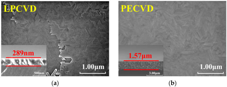
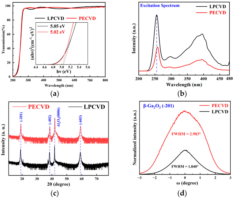
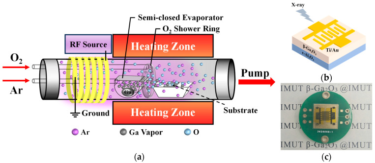
Ultra-wide bandgap β-Ga2O3 is a promising low-cost alternative to conventional direct X-ray detector materials that are limited by fabrication complexity, instability, or slow temporal response. Here, we comparatively investigate β-Ga2O3 thin films grown on c-sapphire by low-pressure chemical vapor deposition (LPCVD) and plasma-enhanced CVD (PECVD), establishing a quantitative linkage between growth kinetics, microstructure, defect landscape, and X-ray detection figures of merit. The LPCVD-grown film (thickness ≈ 0.289 μm) exhibits layered coalesced grains, a narrower rocking curve (FWHM = 1.840°), and deep-level oxygen-vacancy-assisted high photoconductive gain, yielding a high sensitivity of 1.02 × 10⁵ μC Gyair-1 cm-2 at 20 V and a thickness-normalized sensitivity of 3.539 × 10⁵ μCGyair-1 cm-2 μm-1. In contrast, the PECVD-grown film (≈1.57 μm) shows dense columnar growth, higher O/Ga stoichiometric proximity, and shallow-trap dominance, enabling a lower dark current, superior dose detection limit (30.13 vs. 57.07 nGyair s-1), faster recovery, and monotonic SNR improvement with bias. XPS and dual exponential transient analysis corroborate a deep-trap persistent photoconductivity mechanism in LPCVD versus moderated shallow trapping in PECVD. The resulting high-gain vs. low-noise complementary paradigm clarifies defect-gain trade spaces and provides a route to engineer β-Ga2O3 thin-film X-ray detectors that simultaneously target high sensitivity, low dose limit, and temporal stability through trap and electric field management.
期刊介绍:
Nanomaterials (ISSN 2076-4991) is an international and interdisciplinary scholarly open access journal. It publishes reviews, regular research papers, communications, and short notes that are relevant to any field of study that involves nanomaterials, with respect to their science and application. Thus, theoretical and experimental articles will be accepted, along with articles that deal with the synthesis and use of nanomaterials. Articles that synthesize information from multiple fields, and which place discoveries within a broader context, will be preferred. There is no restriction on the length of the papers. Our aim is to encourage scientists to publish their experimental and theoretical research in as much detail as possible. Full experimental or methodical details, or both, must be provided for research articles. Computed data or files regarding the full details of the experimental procedure, if unable to be published in a normal way, can be deposited as supplementary material. Nanomaterials is dedicated to a high scientific standard. All manuscripts undergo a rigorous reviewing process and decisions are based on the recommendations of independent reviewers.

 求助内容:
求助内容: 应助结果提醒方式:


