不同氧流量下双有源层结构对InSnZnO薄膜晶体管性能的增强
IF 3.1
4区 工程技术
Q2 ENGINEERING, ELECTRICAL & ELECTRONIC
引用次数: 0
摘要
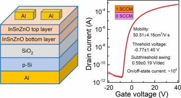
氧化薄膜晶体管(TFTs)已成为高分辨率显示器中应用前景广阔的晶体管之一。不幸的是,它们的电性能,特别是迁移率,受到活性层中氧相关缺陷的限制。本研究采用溅射氧策略的同质结双有源层结构来提高InSnZnO (ITZO) tft的电学性能。通过调节氧气流量,实现不同氧含量的ITZO双活性层的连续溅射。研究了氧对ITZO TFTs电性能的影响。随着氧含量的增加,迁移率降低,而阈值电压升高。由不同氧含量的ITZO薄膜组成的双活性层结构显著提高了迁移率。该双层ITZO TFT具有优良的性能,迁移率为50.51±4.16 cm2/V·s,亚阈值摆幅为0.59±0.19 V/dec,阈值电压为- 0.77±1.40 V,关断电流为- 10−12 a,开/关电流比大于108。研究了ITZO TFTs的栅偏置应力稳定性。在负偏置应力下,当氧流量从1 SCCM增加到7 SCCM时,单层TFTs的阈值电压位移从−14 V提高到−8 V。在偏置应力作用下,双层TFTs表现出合理的阈值电压偏移。这项工作表明,ITZO tft在下一代电子应用中表现出巨大的潜力。本文章由计算机程序翻译,如有差异,请以英文原文为准。
Performance enhancement of InSnZnO thin-film transistors by dual-active-layer architecture with various oxygen flow rates
Oxide thin film transistors (TFTs) have been one of the promising transistors in high-resolution displays. Unfortunately, their electrical performance, especially mobility, is limited by oxygen related defects in the active layers. Here, a homojunction dual-active-layer architecture using sputtering oxygen strategy is employed to enhance the electrical performance of InSnZnO (ITZO) TFTs. The ITZO dual active layers with varying oxygen contents are sequentially sputtered by adjusting the oxygen gas flow rate. The oxygen effects on the electrical performance of the ITZO TFTs are investigated. As the oxygen content increases, the mobility decreases while the threshold voltage increases. The dual-active-layer architecture, composed of ITZO films with varying oxygen contents, significantly improves the mobility. The dual-layer ITZO TFT shows excellent performance with a mobility of 50.51 ± 4.16 cm2/V·s, a subthreshold swing of 0.59 ± 0.19 V/dec, a threshold voltage of −0.77 ± 1.40 V, an off-state current of ∼10−12 A, and an on/off-state current ratio of more than 108. The gate bias stress stability of the ITZO TFTs is investigated. Under negative bias stress, the threshold voltage shift in single-layer TFTs improves from −14 to −8 V as the oxygen flow rate increases from 1 to 7 SCCM. The dual-layer TFTs show a reasonable threshold voltage shift under bias stress. This work demonstrates that the ITZO TFTs exhibit great potential for next-generation electronic applications.
求助全文
通过发布文献求助,成功后即可免费获取论文全文。
去求助
来源期刊

Microelectronic Engineering
工程技术-工程:电子与电气
CiteScore
5.30
自引率
4.30%
发文量
131
审稿时长
29 days
期刊介绍:
Microelectronic Engineering is the premier nanoprocessing, and nanotechnology journal focusing on fabrication of electronic, photonic, bioelectronic, electromechanic and fluidic devices and systems, and their applications in the broad areas of electronics, photonics, energy, life sciences, and environment. It covers also the expanding interdisciplinary field of "more than Moore" and "beyond Moore" integrated nanoelectronics / photonics and micro-/nano-/bio-systems. Through its unique mixture of peer-reviewed articles, reviews, accelerated publications, short and Technical notes, and the latest research news on key developments, Microelectronic Engineering provides comprehensive coverage of this exciting, interdisciplinary and dynamic new field for researchers in academia and professionals in industry.
 求助内容:
求助内容: 应助结果提醒方式:


