{"title":"提高集成电路制造性能的高阶先进光刻叠加校正方法。","authors":"Dinghai Rui, Libin Zhang, Yayi Wei and Yajuan Su","doi":"10.1039/D5NA00682A","DOIUrl":null,"url":null,"abstract":"<p >As integrated circuit (IC) manufacturing advances toward smaller technology nodes, conventional lithography methods are increasingly challenged by the diffraction-limited resolution, escalating process complexity, and rising costs. Among these challenges, overlays have a particularly pronounced impact on manufacturing quality. To address this issue, this paper proposes a high-order overlay correction model that employs a two-dimensional fifth-order polynomial to accurately fit and characterize the distribution of overlays. The model's effectiveness is validated through finite element simulations. By incorporating an array of piezoelectric actuators, thermally induced deformation control units, and micro-mechanical clamping mechanisms, the model enables precise regulation of complex stress fields and localized temperature variations along the mask boundary, thereby enabling effective compensation of high-order overlay errors. Simulation results demonstrate that the proposed approach reduces the |mean| + 3<em>σ</em> of overlay to below 1 nm. It achieves nearly 100% correction for 1st-order and 2nd-order overlay components, over 80% correction for 3rd-order and 4th-order components, and a correction rate of 68.16% for 5th-order errors. Multiple randomized verification tests indicate average compensation efficiencies of 96.85% in the <em>x</em>-direction and 97.36% in the <em>y</em>-direction, highlighting the model's robustness and consistency. In practical processes, the model successfully reduces actual wafer overlay to |mean| + 3<em>σ</em> values of 4.22 nm and 6.26 nm in the <em>x</em> and <em>y</em> directions, respectively. This study presents an efficient and reliable solution for high-order overlay compensation in advanced lithography, offering significant benefits for enhancing IC manufacturing performance and reliability.</p>","PeriodicalId":18806,"journal":{"name":"Nanoscale Advances","volume":" 20","pages":" 6563-6574"},"PeriodicalIF":4.6000,"publicationDate":"2025-09-05","publicationTypes":"Journal Article","fieldsOfStudy":null,"isOpenAccess":false,"openAccessPdf":"https://www.ncbi.nlm.nih.gov/pmc/articles/PMC12412054/pdf/","citationCount":"0","resultStr":"{\"title\":\"Method of high-order advanced lithography overlay correction to enhance the manufacturing performance of integrated circuits\",\"authors\":\"Dinghai Rui, Libin Zhang, Yayi Wei and Yajuan Su\",\"doi\":\"10.1039/D5NA00682A\",\"DOIUrl\":null,\"url\":null,\"abstract\":\"<p >As integrated circuit (IC) manufacturing advances toward smaller technology nodes, conventional lithography methods are increasingly challenged by the diffraction-limited resolution, escalating process complexity, and rising costs. Among these challenges, overlays have a particularly pronounced impact on manufacturing quality. To address this issue, this paper proposes a high-order overlay correction model that employs a two-dimensional fifth-order polynomial to accurately fit and characterize the distribution of overlays. The model's effectiveness is validated through finite element simulations. By incorporating an array of piezoelectric actuators, thermally induced deformation control units, and micro-mechanical clamping mechanisms, the model enables precise regulation of complex stress fields and localized temperature variations along the mask boundary, thereby enabling effective compensation of high-order overlay errors. Simulation results demonstrate that the proposed approach reduces the |mean| + 3<em>σ</em> of overlay to below 1 nm. It achieves nearly 100% correction for 1st-order and 2nd-order overlay components, over 80% correction for 3rd-order and 4th-order components, and a correction rate of 68.16% for 5th-order errors. Multiple randomized verification tests indicate average compensation efficiencies of 96.85% in the <em>x</em>-direction and 97.36% in the <em>y</em>-direction, highlighting the model's robustness and consistency. In practical processes, the model successfully reduces actual wafer overlay to |mean| + 3<em>σ</em> values of 4.22 nm and 6.26 nm in the <em>x</em> and <em>y</em> directions, respectively. This study presents an efficient and reliable solution for high-order overlay compensation in advanced lithography, offering significant benefits for enhancing IC manufacturing performance and reliability.</p>\",\"PeriodicalId\":18806,\"journal\":{\"name\":\"Nanoscale Advances\",\"volume\":\" 20\",\"pages\":\" 6563-6574\"},\"PeriodicalIF\":4.6000,\"publicationDate\":\"2025-09-05\",\"publicationTypes\":\"Journal Article\",\"fieldsOfStudy\":null,\"isOpenAccess\":false,\"openAccessPdf\":\"https://www.ncbi.nlm.nih.gov/pmc/articles/PMC12412054/pdf/\",\"citationCount\":\"0\",\"resultStr\":null,\"platform\":\"Semanticscholar\",\"paperid\":null,\"PeriodicalName\":\"Nanoscale Advances\",\"FirstCategoryId\":\"88\",\"ListUrlMain\":\"https://pubs.rsc.org/en/content/articlelanding/2025/na/d5na00682a\",\"RegionNum\":3,\"RegionCategory\":\"材料科学\",\"ArticlePicture\":[],\"TitleCN\":null,\"AbstractTextCN\":null,\"PMCID\":null,\"EPubDate\":\"\",\"PubModel\":\"\",\"JCR\":\"Q2\",\"JCRName\":\"CHEMISTRY, MULTIDISCIPLINARY\",\"Score\":null,\"Total\":0}","platform":"Semanticscholar","paperid":null,"PeriodicalName":"Nanoscale Advances","FirstCategoryId":"88","ListUrlMain":"https://pubs.rsc.org/en/content/articlelanding/2025/na/d5na00682a","RegionNum":3,"RegionCategory":"材料科学","ArticlePicture":[],"TitleCN":null,"AbstractTextCN":null,"PMCID":null,"EPubDate":"","PubModel":"","JCR":"Q2","JCRName":"CHEMISTRY, MULTIDISCIPLINARY","Score":null,"Total":0}
Method of high-order advanced lithography overlay correction to enhance the manufacturing performance of integrated circuits
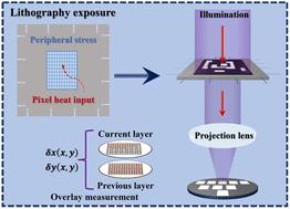
As integrated circuit (IC) manufacturing advances toward smaller technology nodes, conventional lithography methods are increasingly challenged by the diffraction-limited resolution, escalating process complexity, and rising costs. Among these challenges, overlays have a particularly pronounced impact on manufacturing quality. To address this issue, this paper proposes a high-order overlay correction model that employs a two-dimensional fifth-order polynomial to accurately fit and characterize the distribution of overlays. The model's effectiveness is validated through finite element simulations. By incorporating an array of piezoelectric actuators, thermally induced deformation control units, and micro-mechanical clamping mechanisms, the model enables precise regulation of complex stress fields and localized temperature variations along the mask boundary, thereby enabling effective compensation of high-order overlay errors. Simulation results demonstrate that the proposed approach reduces the |mean| + 3σ of overlay to below 1 nm. It achieves nearly 100% correction for 1st-order and 2nd-order overlay components, over 80% correction for 3rd-order and 4th-order components, and a correction rate of 68.16% for 5th-order errors. Multiple randomized verification tests indicate average compensation efficiencies of 96.85% in the x-direction and 97.36% in the y-direction, highlighting the model's robustness and consistency. In practical processes, the model successfully reduces actual wafer overlay to |mean| + 3σ values of 4.22 nm and 6.26 nm in the x and y directions, respectively. This study presents an efficient and reliable solution for high-order overlay compensation in advanced lithography, offering significant benefits for enhancing IC manufacturing performance and reliability.

 求助内容:
求助内容: 应助结果提醒方式:


