使用O3钝化I/O器件提高堆叠SiGe/Si finfet的电气性能和可靠性
IF 3.1
4区 工程技术
Q2 ENGINEERING, ELECTRICAL & ELECTRONIC
引用次数: 0
摘要
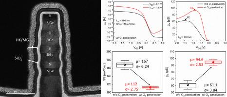
在这项工作中,研究了新型堆叠SiGe/Si FinFET输入输出(I/O)器件的O3钝化技术。首先,验证了基于SiGe MOS电容(CAP)结构的O3钝化技术。,结果表明,界面态密度(Dit)可降至5.12 × 10¹² eV−1 cm−2。然后,为了提高堆叠型SiGe/Si FinFET I/O器件的电学性能,在SiGe/Si鳍片与栅极氧化物之间引入O3钝化技术。因此,堆叠的SiGe/Si FinFET I/O器件的电学性能得到了显著改善。SS从168 mV/dec降低到113 mV/dec, gm从62 μS提高到94 μS,这主要是由于O3钝化导致Dit的降低。并对其进行了可靠性评估。结果表明,在负偏置温度不稳定性(NBTI)和热载流子注入(HCI)应力下,阈值电压(VTH)漂移分别提高了52.1%和60.3%。同时,在故障率为0.01%的情况下,其10年寿命的最大工作电压(Vmax)可达2.65 V。因此,O3钝化工艺对于先进GAA平台上堆叠的SiGe/Si I/O FinFET器件是实用的。本文章由计算机程序翻译,如有差异,请以英文原文为准。
Improving electrical performance and reliability of stacked SiGe/Si FinFETs using O3 passivation for I/O devices
In this work, O3 passivation technology for the novel stacked SiGe/Si FinFET input-output (I/O) devices was investigated. First, the O3 passivation technology was validated based on SiGe MOS capacitance (CAP) structure., with results indicating that interface state density (Dit) can be reduced to 5.12 × 10¹² eV−1 cm−2. Then, to improve the electrical performance of the stacked SiGe/Si FinFET I/O device, the O3 passivation technology was introduced between the SiGe/Si fin and gate oxide. As a result, the electrical performance for the stacked SiGe/Si FinFET I/O device was significantly improved. For example, SS could be reduced from the 168 mV/dec to 113 mV/dec, and gm could be improved from the 62 μS to 94 μS, which was mainly attributed to the O3 passivation resulting in the reduction of Dit. Furthermore, its reliability assessment was also performed. The result confirmed that threshold voltage (VTH) drift under negative bias temperature instability (NBTI) and hot carrier injection (HCI) stress were improved by 52.1 % and 60.3 %, respectively. Meanwhile, its maximum operating voltage (Vmax) for a 10 years lifetime at a failure rate of 0.01 % could reach to 2.65 V. Therefore, the O3 passivation process is practical for the stacked SiGe/Si I/O FinFET device in advanced GAA platforms.
求助全文
通过发布文献求助,成功后即可免费获取论文全文。
去求助
来源期刊

Microelectronic Engineering
工程技术-工程:电子与电气
CiteScore
5.30
自引率
4.30%
发文量
131
审稿时长
29 days
期刊介绍:
Microelectronic Engineering is the premier nanoprocessing, and nanotechnology journal focusing on fabrication of electronic, photonic, bioelectronic, electromechanic and fluidic devices and systems, and their applications in the broad areas of electronics, photonics, energy, life sciences, and environment. It covers also the expanding interdisciplinary field of "more than Moore" and "beyond Moore" integrated nanoelectronics / photonics and micro-/nano-/bio-systems. Through its unique mixture of peer-reviewed articles, reviews, accelerated publications, short and Technical notes, and the latest research news on key developments, Microelectronic Engineering provides comprehensive coverage of this exciting, interdisciplinary and dynamic new field for researchers in academia and professionals in industry.
 求助内容:
求助内容: 应助结果提醒方式:


