Gour Mohan Das, Eero Hulkko, Pasi Myllyperkiö, Andreas Johansson, Mika Pettersson
{"title":"石墨烯的近场光学纳米图。","authors":"Gour Mohan Das, Eero Hulkko, Pasi Myllyperkiö, Andreas Johansson, Mika Pettersson","doi":"10.1002/smsc.202500184","DOIUrl":null,"url":null,"abstract":"<p><p>2D materials are emerging as transformative platforms for next-generation memory, sensing, photonic, and quantum devices due to their extraordinary optical, mechanical, and electronic properties. A key challenge is achieving controlled and precise nanopatterning to unlock tailored functionalities. This work uses a direct laser writing method to introduce a near-field-mediated nanopatterning technique that delivers ≈10-30 nm lateral and sub-5 nm vertical modification on graphene under ambient conditions. This approach uses a pulsed femtosecond laser in the visible wavelength range with scattering-type scanning near-field optical microscopy (s-SNOM), where the s-SNOM tip serves as a nanoscale probe. The resultant nanopatterns exhibit highly symmetric, periodic nanoscale holes with spherical perforations (nanopunch holes), with 5-25 nm dimensions. Importantly, nano- Fourier transform infrared spectroscopy reveals selective oxidative functionalization at the periphery of the nanopunch holes, highlighting a controlled surface modification of graphene. By finely tuning experimental parameters such as laser exposure time, the nanopatterning feature size ranging from 1-30 nm, and the resulting shapes from nanoscale elevated structures (nanoblister shape) to punched holes can be precisely modulated. This nanopatterning strategy achieves feature sizes at the sub-10 nm scale and represents an advancement toward fabricating all-2D material devices, setting new benchmark in nanoscale manufacturing for quantum and photonic technologies.</p>","PeriodicalId":29791,"journal":{"name":"Small Science","volume":"5 8","pages":"2500184"},"PeriodicalIF":8.3000,"publicationDate":"2025-06-30","publicationTypes":"Journal Article","fieldsOfStudy":null,"isOpenAccess":false,"openAccessPdf":"https://www.ncbi.nlm.nih.gov/pmc/articles/PMC12362822/pdf/","citationCount":"0","resultStr":"{\"title\":\"Near-Field Optical Nanopatterning of Graphene.\",\"authors\":\"Gour Mohan Das, Eero Hulkko, Pasi Myllyperkiö, Andreas Johansson, Mika Pettersson\",\"doi\":\"10.1002/smsc.202500184\",\"DOIUrl\":null,\"url\":null,\"abstract\":\"<p><p>2D materials are emerging as transformative platforms for next-generation memory, sensing, photonic, and quantum devices due to their extraordinary optical, mechanical, and electronic properties. A key challenge is achieving controlled and precise nanopatterning to unlock tailored functionalities. This work uses a direct laser writing method to introduce a near-field-mediated nanopatterning technique that delivers ≈10-30 nm lateral and sub-5 nm vertical modification on graphene under ambient conditions. This approach uses a pulsed femtosecond laser in the visible wavelength range with scattering-type scanning near-field optical microscopy (s-SNOM), where the s-SNOM tip serves as a nanoscale probe. The resultant nanopatterns exhibit highly symmetric, periodic nanoscale holes with spherical perforations (nanopunch holes), with 5-25 nm dimensions. Importantly, nano- Fourier transform infrared spectroscopy reveals selective oxidative functionalization at the periphery of the nanopunch holes, highlighting a controlled surface modification of graphene. By finely tuning experimental parameters such as laser exposure time, the nanopatterning feature size ranging from 1-30 nm, and the resulting shapes from nanoscale elevated structures (nanoblister shape) to punched holes can be precisely modulated. This nanopatterning strategy achieves feature sizes at the sub-10 nm scale and represents an advancement toward fabricating all-2D material devices, setting new benchmark in nanoscale manufacturing for quantum and photonic technologies.</p>\",\"PeriodicalId\":29791,\"journal\":{\"name\":\"Small Science\",\"volume\":\"5 8\",\"pages\":\"2500184\"},\"PeriodicalIF\":8.3000,\"publicationDate\":\"2025-06-30\",\"publicationTypes\":\"Journal Article\",\"fieldsOfStudy\":null,\"isOpenAccess\":false,\"openAccessPdf\":\"https://www.ncbi.nlm.nih.gov/pmc/articles/PMC12362822/pdf/\",\"citationCount\":\"0\",\"resultStr\":null,\"platform\":\"Semanticscholar\",\"paperid\":null,\"PeriodicalName\":\"Small Science\",\"FirstCategoryId\":\"1085\",\"ListUrlMain\":\"https://doi.org/10.1002/smsc.202500184\",\"RegionNum\":0,\"RegionCategory\":null,\"ArticlePicture\":[],\"TitleCN\":null,\"AbstractTextCN\":null,\"PMCID\":null,\"EPubDate\":\"2025/8/1 0:00:00\",\"PubModel\":\"eCollection\",\"JCR\":\"Q1\",\"JCRName\":\"MATERIALS SCIENCE, MULTIDISCIPLINARY\",\"Score\":null,\"Total\":0}","platform":"Semanticscholar","paperid":null,"PeriodicalName":"Small Science","FirstCategoryId":"1085","ListUrlMain":"https://doi.org/10.1002/smsc.202500184","RegionNum":0,"RegionCategory":null,"ArticlePicture":[],"TitleCN":null,"AbstractTextCN":null,"PMCID":null,"EPubDate":"2025/8/1 0:00:00","PubModel":"eCollection","JCR":"Q1","JCRName":"MATERIALS SCIENCE, MULTIDISCIPLINARY","Score":null,"Total":0}
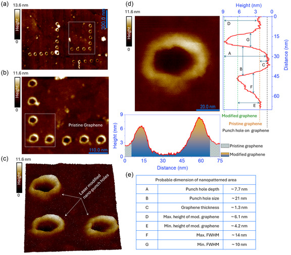
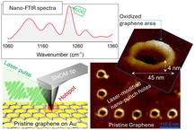
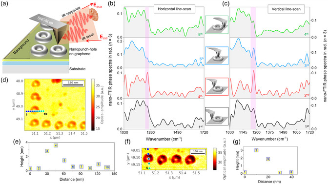
2D materials are emerging as transformative platforms for next-generation memory, sensing, photonic, and quantum devices due to their extraordinary optical, mechanical, and electronic properties. A key challenge is achieving controlled and precise nanopatterning to unlock tailored functionalities. This work uses a direct laser writing method to introduce a near-field-mediated nanopatterning technique that delivers ≈10-30 nm lateral and sub-5 nm vertical modification on graphene under ambient conditions. This approach uses a pulsed femtosecond laser in the visible wavelength range with scattering-type scanning near-field optical microscopy (s-SNOM), where the s-SNOM tip serves as a nanoscale probe. The resultant nanopatterns exhibit highly symmetric, periodic nanoscale holes with spherical perforations (nanopunch holes), with 5-25 nm dimensions. Importantly, nano- Fourier transform infrared spectroscopy reveals selective oxidative functionalization at the periphery of the nanopunch holes, highlighting a controlled surface modification of graphene. By finely tuning experimental parameters such as laser exposure time, the nanopatterning feature size ranging from 1-30 nm, and the resulting shapes from nanoscale elevated structures (nanoblister shape) to punched holes can be precisely modulated. This nanopatterning strategy achieves feature sizes at the sub-10 nm scale and represents an advancement toward fabricating all-2D material devices, setting new benchmark in nanoscale manufacturing for quantum and photonic technologies.
期刊介绍:
Small Science is a premium multidisciplinary open access journal dedicated to publishing impactful research from all areas of nanoscience and nanotechnology. It features interdisciplinary original research and focused review articles on relevant topics. The journal covers design, characterization, mechanism, technology, and application of micro-/nanoscale structures and systems in various fields including physics, chemistry, materials science, engineering, environmental science, life science, biology, and medicine. It welcomes innovative interdisciplinary research and its readership includes professionals from academia and industry in fields such as chemistry, physics, materials science, biology, engineering, and environmental and analytical science. Small Science is indexed and abstracted in CAS, DOAJ, Clarivate Analytics, ProQuest Central, Publicly Available Content Database, Science Database, SCOPUS, and Web of Science.

 求助内容:
求助内容: 应助结果提醒方式:


