Alexander V. Rumyantsev, Nikolai I. Borgardt and Roman L. Volkov
{"title":"聚焦离子束纳米加工中的还原离子注入","authors":"Alexander V. Rumyantsev, Nikolai I. Borgardt and Roman L. Volkov","doi":"10.1039/D5NR01571E","DOIUrl":null,"url":null,"abstract":"<p >The focused ion beam (FIB) technique has been established as a powerful nanofabrication tool. The application of this technique is limited due to the implantation of beam ions into the substrate, which is difficult to overcome and can be detrimental in many cases. Herein, we report that in comparison with the commonly used smooth milling process, the amount of implanted gallium atoms in the near-surface region of fabricated structures can be significantly reduced when the ions strike a highly inclined sputtering front wall formed on the substrate surface during the edge milling process of the line-by-line beam scanning strategy. To justify this conclusion, a set of test structures of rectangular boxes were prepared using the line-by-line scanning strategy of gallium FIB in a silicon substrate, and their cross-sectional specimens were examined by transmission electron microscopy technique and energy-dispersive X-ray microanalysis. It was demonstrated that the transition from smooth to edge milling processes resulted in a decrease in the maximum concentration of implanted gallium atoms from approximately 45 to 15 at% for boxes with depths of 81 and 300 nm, respectively. The developed theoretical approach allowed to predict the shape of the boxes and qualitatively estimate their depth as well as the concentration of the implanted gallium atoms. Monte Carlo simulations indicated that the removal of secondary material by sputtered silicon atoms played a significant role in reducing the concentration of implanted gallium atoms. The results of this study provide a way to significantly improve the quality of FIB-fabricated structures for various applications.</p>","PeriodicalId":92,"journal":{"name":"Nanoscale","volume":" 36","pages":" 21141-21156"},"PeriodicalIF":5.1000,"publicationDate":"2025-09-01","publicationTypes":"Journal Article","fieldsOfStudy":null,"isOpenAccess":false,"openAccessPdf":"","citationCount":"0","resultStr":"{\"title\":\"Reducing ion implantation in focused ion beam nanofabrication\",\"authors\":\"Alexander V. Rumyantsev, Nikolai I. Borgardt and Roman L. Volkov\",\"doi\":\"10.1039/D5NR01571E\",\"DOIUrl\":null,\"url\":null,\"abstract\":\"<p >The focused ion beam (FIB) technique has been established as a powerful nanofabrication tool. The application of this technique is limited due to the implantation of beam ions into the substrate, which is difficult to overcome and can be detrimental in many cases. Herein, we report that in comparison with the commonly used smooth milling process, the amount of implanted gallium atoms in the near-surface region of fabricated structures can be significantly reduced when the ions strike a highly inclined sputtering front wall formed on the substrate surface during the edge milling process of the line-by-line beam scanning strategy. To justify this conclusion, a set of test structures of rectangular boxes were prepared using the line-by-line scanning strategy of gallium FIB in a silicon substrate, and their cross-sectional specimens were examined by transmission electron microscopy technique and energy-dispersive X-ray microanalysis. It was demonstrated that the transition from smooth to edge milling processes resulted in a decrease in the maximum concentration of implanted gallium atoms from approximately 45 to 15 at% for boxes with depths of 81 and 300 nm, respectively. The developed theoretical approach allowed to predict the shape of the boxes and qualitatively estimate their depth as well as the concentration of the implanted gallium atoms. Monte Carlo simulations indicated that the removal of secondary material by sputtered silicon atoms played a significant role in reducing the concentration of implanted gallium atoms. The results of this study provide a way to significantly improve the quality of FIB-fabricated structures for various applications.</p>\",\"PeriodicalId\":92,\"journal\":{\"name\":\"Nanoscale\",\"volume\":\" 36\",\"pages\":\" 21141-21156\"},\"PeriodicalIF\":5.1000,\"publicationDate\":\"2025-09-01\",\"publicationTypes\":\"Journal Article\",\"fieldsOfStudy\":null,\"isOpenAccess\":false,\"openAccessPdf\":\"\",\"citationCount\":\"0\",\"resultStr\":null,\"platform\":\"Semanticscholar\",\"paperid\":null,\"PeriodicalName\":\"Nanoscale\",\"FirstCategoryId\":\"88\",\"ListUrlMain\":\"https://pubs.rsc.org/en/content/articlelanding/2025/nr/d5nr01571e\",\"RegionNum\":3,\"RegionCategory\":\"材料科学\",\"ArticlePicture\":[],\"TitleCN\":null,\"AbstractTextCN\":null,\"PMCID\":null,\"EPubDate\":\"\",\"PubModel\":\"\",\"JCR\":\"Q1\",\"JCRName\":\"CHEMISTRY, MULTIDISCIPLINARY\",\"Score\":null,\"Total\":0}","platform":"Semanticscholar","paperid":null,"PeriodicalName":"Nanoscale","FirstCategoryId":"88","ListUrlMain":"https://pubs.rsc.org/en/content/articlelanding/2025/nr/d5nr01571e","RegionNum":3,"RegionCategory":"材料科学","ArticlePicture":[],"TitleCN":null,"AbstractTextCN":null,"PMCID":null,"EPubDate":"","PubModel":"","JCR":"Q1","JCRName":"CHEMISTRY, MULTIDISCIPLINARY","Score":null,"Total":0}
Reducing ion implantation in focused ion beam nanofabrication
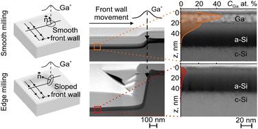
The focused ion beam (FIB) technique has been established as a powerful nanofabrication tool. The application of this technique is limited due to the implantation of beam ions into the substrate, which is difficult to overcome and can be detrimental in many cases. Herein, we report that in comparison with the commonly used smooth milling process, the amount of implanted gallium atoms in the near-surface region of fabricated structures can be significantly reduced when the ions strike a highly inclined sputtering front wall formed on the substrate surface during the edge milling process of the line-by-line beam scanning strategy. To justify this conclusion, a set of test structures of rectangular boxes were prepared using the line-by-line scanning strategy of gallium FIB in a silicon substrate, and their cross-sectional specimens were examined by transmission electron microscopy technique and energy-dispersive X-ray microanalysis. It was demonstrated that the transition from smooth to edge milling processes resulted in a decrease in the maximum concentration of implanted gallium atoms from approximately 45 to 15 at% for boxes with depths of 81 and 300 nm, respectively. The developed theoretical approach allowed to predict the shape of the boxes and qualitatively estimate their depth as well as the concentration of the implanted gallium atoms. Monte Carlo simulations indicated that the removal of secondary material by sputtered silicon atoms played a significant role in reducing the concentration of implanted gallium atoms. The results of this study provide a way to significantly improve the quality of FIB-fabricated structures for various applications.
期刊介绍:
Nanoscale is a high-impact international journal, publishing high-quality research across nanoscience and nanotechnology. Nanoscale publishes a full mix of research articles on experimental and theoretical work, including reviews, communications, and full papers.Highly interdisciplinary, this journal appeals to scientists, researchers and professionals interested in nanoscience and nanotechnology, quantum materials and quantum technology, including the areas of physics, chemistry, biology, medicine, materials, energy/environment, information technology, detection science, healthcare and drug discovery, and electronics.


 求助内容:
求助内容: 应助结果提醒方式:


