Nathan Aubergier, Vincent T. Renard, Sylvain Barraud, Kei Takashina and Benjamin A. Piot*,
{"title":"双门控绝缘体上硅量子阱中谷分裂的宽电可调性","authors":"Nathan Aubergier, Vincent T. Renard, Sylvain Barraud, Kei Takashina and Benjamin A. Piot*, ","doi":"10.1021/acs.nanolett.5c03049","DOIUrl":null,"url":null,"abstract":"<p >The valley splitting of 2D electrons in doubly gated silicon-on-insulator quantum wells is studied by low temperature transport measurements under magnetic fields. At the buried thermal-oxide SiO<sub>2</sub> interface, the valley splitting increases as a function of the electrostatic bias <i>δn</i> = <i>n</i><sub><i>B</i></sub> – <i>n</i><sub><i>F</i></sub> (where <i>n</i><sub><i>B</i></sub> and <i>n</i><sub><i>F</i></sub> are electron densities contributed by back and front gates, respectively) and reaches values as high as 6.3 meV, independent of the total carrier concentration of the channel. We show that <i>δn</i> tunes the square of the wave function modulus at the interface and its penetration into the barrier, both of which are key quantities in a theory describing interface-induced valley splitting, and is therefore the natural experimental parameter to manipulate valleys in 2D silicon systems. At the front interface, made of a thin “high-k” dielectric, a smaller valley splitting is observed, adding further options to tune the valley splitting within a single device.</p>","PeriodicalId":53,"journal":{"name":"Nano Letters","volume":"25 36","pages":"13557–13562"},"PeriodicalIF":9.1000,"publicationDate":"2025-08-27","publicationTypes":"Journal Article","fieldsOfStudy":null,"isOpenAccess":false,"openAccessPdf":"","citationCount":"0","resultStr":"{\"title\":\"Wide Electrical Tunability of the Valley Splitting in a Doubly Gated Silicon-on-Insulator Quantum Well\",\"authors\":\"Nathan Aubergier, Vincent T. Renard, Sylvain Barraud, Kei Takashina and Benjamin A. Piot*, \",\"doi\":\"10.1021/acs.nanolett.5c03049\",\"DOIUrl\":null,\"url\":null,\"abstract\":\"<p >The valley splitting of 2D electrons in doubly gated silicon-on-insulator quantum wells is studied by low temperature transport measurements under magnetic fields. At the buried thermal-oxide SiO<sub>2</sub> interface, the valley splitting increases as a function of the electrostatic bias <i>δn</i> = <i>n</i><sub><i>B</i></sub> – <i>n</i><sub><i>F</i></sub> (where <i>n</i><sub><i>B</i></sub> and <i>n</i><sub><i>F</i></sub> are electron densities contributed by back and front gates, respectively) and reaches values as high as 6.3 meV, independent of the total carrier concentration of the channel. We show that <i>δn</i> tunes the square of the wave function modulus at the interface and its penetration into the barrier, both of which are key quantities in a theory describing interface-induced valley splitting, and is therefore the natural experimental parameter to manipulate valleys in 2D silicon systems. At the front interface, made of a thin “high-k” dielectric, a smaller valley splitting is observed, adding further options to tune the valley splitting within a single device.</p>\",\"PeriodicalId\":53,\"journal\":{\"name\":\"Nano Letters\",\"volume\":\"25 36\",\"pages\":\"13557–13562\"},\"PeriodicalIF\":9.1000,\"publicationDate\":\"2025-08-27\",\"publicationTypes\":\"Journal Article\",\"fieldsOfStudy\":null,\"isOpenAccess\":false,\"openAccessPdf\":\"\",\"citationCount\":\"0\",\"resultStr\":null,\"platform\":\"Semanticscholar\",\"paperid\":null,\"PeriodicalName\":\"Nano Letters\",\"FirstCategoryId\":\"88\",\"ListUrlMain\":\"https://pubs.acs.org/doi/10.1021/acs.nanolett.5c03049\",\"RegionNum\":1,\"RegionCategory\":\"材料科学\",\"ArticlePicture\":[],\"TitleCN\":null,\"AbstractTextCN\":null,\"PMCID\":null,\"EPubDate\":\"\",\"PubModel\":\"\",\"JCR\":\"Q1\",\"JCRName\":\"CHEMISTRY, MULTIDISCIPLINARY\",\"Score\":null,\"Total\":0}","platform":"Semanticscholar","paperid":null,"PeriodicalName":"Nano Letters","FirstCategoryId":"88","ListUrlMain":"https://pubs.acs.org/doi/10.1021/acs.nanolett.5c03049","RegionNum":1,"RegionCategory":"材料科学","ArticlePicture":[],"TitleCN":null,"AbstractTextCN":null,"PMCID":null,"EPubDate":"","PubModel":"","JCR":"Q1","JCRName":"CHEMISTRY, MULTIDISCIPLINARY","Score":null,"Total":0}
引用次数: 0
摘要
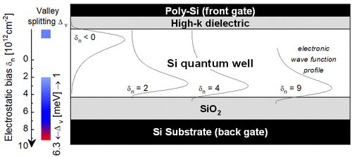
利用磁场下的低温输运测量研究了双门控绝缘体上硅量子阱中二维电子的谷分裂。在埋置的热氧化物SiO2界面上,谷分裂随着静电偏压δn = nB - nF(其中nB和nF分别为前后栅极贡献的电子密度)的增加而增加,并达到高达6.3 meV的值,与通道的总载流子浓度无关。我们发现δn调节了界面处波函数模量的平方及其对势垒的渗透,这两者都是描述界面诱导谷分裂理论的关键量,因此是操纵二维硅系统中谷的自然实验参数。在前界面,由薄的“高k”电介质制成,观察到较小的谷分裂,增加了在单个器件内调整谷分裂的进一步选择。
Wide Electrical Tunability of the Valley Splitting in a Doubly Gated Silicon-on-Insulator Quantum Well
The valley splitting of 2D electrons in doubly gated silicon-on-insulator quantum wells is studied by low temperature transport measurements under magnetic fields. At the buried thermal-oxide SiO2 interface, the valley splitting increases as a function of the electrostatic bias δn = nB – nF (where nB and nF are electron densities contributed by back and front gates, respectively) and reaches values as high as 6.3 meV, independent of the total carrier concentration of the channel. We show that δn tunes the square of the wave function modulus at the interface and its penetration into the barrier, both of which are key quantities in a theory describing interface-induced valley splitting, and is therefore the natural experimental parameter to manipulate valleys in 2D silicon systems. At the front interface, made of a thin “high-k” dielectric, a smaller valley splitting is observed, adding further options to tune the valley splitting within a single device.
期刊介绍:
Nano Letters serves as a dynamic platform for promptly disseminating original results in fundamental, applied, and emerging research across all facets of nanoscience and nanotechnology. A pivotal criterion for inclusion within Nano Letters is the convergence of at least two different areas or disciplines, ensuring a rich interdisciplinary scope. The journal is dedicated to fostering exploration in diverse areas, including:
- Experimental and theoretical findings on physical, chemical, and biological phenomena at the nanoscale
- Synthesis, characterization, and processing of organic, inorganic, polymer, and hybrid nanomaterials through physical, chemical, and biological methodologies
- Modeling and simulation of synthetic, assembly, and interaction processes
- Realization of integrated nanostructures and nano-engineered devices exhibiting advanced performance
- Applications of nanoscale materials in living and environmental systems
Nano Letters is committed to advancing and showcasing groundbreaking research that intersects various domains, fostering innovation and collaboration in the ever-evolving field of nanoscience and nanotechnology.


 求助内容:
求助内容: 应助结果提醒方式:


