基于振镜的准直无误差全原位成像和激光处理系统及其在泛半导体制造中的应用

IF 11.6 1区 工程技术 Q1 ENGINEERING, MULTIDISCIPLINARY
Yuxuan Cao, Kuai Yang, Yingchun Guan, Zhen Zhang
{"title":"基于振镜的准直无误差全原位成像和激光处理系统及其在泛半导体制造中的应用","authors":"Yuxuan Cao, Kuai Yang, Yingchun Guan, Zhen Zhang","doi":"10.1016/j.eng.2025.07.041","DOIUrl":null,"url":null,"abstract":"The non-physical-contact property of lasers poses significant challenges for the alignment procedure in precision engineering. Particularly in galvanometer-based laser processing systems, the requirement for multiple-step coordinate conversion further complicates the alignment procedure, thereby increasing the potential for error accumulation. To address the alignment issues during galvanometer laser scanning, this paper proposes an alignment-error-free solution for full-<em>in-situ</em> imaging and laser processing system, which eliminates the alignment error at the principal level by skipping the coordinate conversion and directly extracting angular coordinates for laser scanning from the captured images. Compared with the existing galvanometer-based laser processing systems, the main advantage of the proposed method is its ability to achieve alignment-error-free without requiring calibration, making it particularly suitable for small-batch, highly customized, and complex processing tasks. This system specifically facilitates in-line inspection, detection, and measurement during laser fabrications. Furthermore, two experimental cases in pan-semiconductor manufacturing, which includes flexible printed circuits (FPC) cutting and Micro-LEDs defect detection, have been conducted to demonstrate the validation of the proposed full-<em>in-situ</em> processing system. Correspondingly, the current experimental comparisons highlight the superiority of the proposed system for simultaneously achieving a maximum range of 27 mm × 27 mm and a minimum resolution of 0.412 µm, with a maximum processing error &lt;15 µm. Demonstrations in detecting and processing the complex patterns illustrate its exceptional capabilities in alignment-error-free laser processing for precision manufacturing.","PeriodicalId":11783,"journal":{"name":"Engineering","volume":"16 1","pages":""},"PeriodicalIF":11.6000,"publicationDate":"2025-08-26","publicationTypes":"Journal Article","fieldsOfStudy":null,"isOpenAccess":false,"openAccessPdf":"","citationCount":"0","resultStr":"{\"title\":\"Galvanometer-Based Alignment-Error-Free Full-in-Situ Imaging and Laser Processing System with Applications to Pan-Semiconductor Manufacturing\",\"authors\":\"Yuxuan Cao, Kuai Yang, Yingchun Guan, Zhen Zhang\",\"doi\":\"10.1016/j.eng.2025.07.041\",\"DOIUrl\":null,\"url\":null,\"abstract\":\"The non-physical-contact property of lasers poses significant challenges for the alignment procedure in precision engineering. Particularly in galvanometer-based laser processing systems, the requirement for multiple-step coordinate conversion further complicates the alignment procedure, thereby increasing the potential for error accumulation. To address the alignment issues during galvanometer laser scanning, this paper proposes an alignment-error-free solution for full-<em>in-situ</em> imaging and laser processing system, which eliminates the alignment error at the principal level by skipping the coordinate conversion and directly extracting angular coordinates for laser scanning from the captured images. Compared with the existing galvanometer-based laser processing systems, the main advantage of the proposed method is its ability to achieve alignment-error-free without requiring calibration, making it particularly suitable for small-batch, highly customized, and complex processing tasks. This system specifically facilitates in-line inspection, detection, and measurement during laser fabrications. Furthermore, two experimental cases in pan-semiconductor manufacturing, which includes flexible printed circuits (FPC) cutting and Micro-LEDs defect detection, have been conducted to demonstrate the validation of the proposed full-<em>in-situ</em> processing system. Correspondingly, the current experimental comparisons highlight the superiority of the proposed system for simultaneously achieving a maximum range of 27 mm × 27 mm and a minimum resolution of 0.412 µm, with a maximum processing error &lt;15 µm. Demonstrations in detecting and processing the complex patterns illustrate its exceptional capabilities in alignment-error-free laser processing for precision manufacturing.\",\"PeriodicalId\":11783,\"journal\":{\"name\":\"Engineering\",\"volume\":\"16 1\",\"pages\":\"\"},\"PeriodicalIF\":11.6000,\"publicationDate\":\"2025-08-26\",\"publicationTypes\":\"Journal Article\",\"fieldsOfStudy\":null,\"isOpenAccess\":false,\"openAccessPdf\":\"\",\"citationCount\":\"0\",\"resultStr\":null,\"platform\":\"Semanticscholar\",\"paperid\":null,\"PeriodicalName\":\"Engineering\",\"FirstCategoryId\":\"5\",\"ListUrlMain\":\"https://doi.org/10.1016/j.eng.2025.07.041\",\"RegionNum\":1,\"RegionCategory\":\"工程技术\",\"ArticlePicture\":[],\"TitleCN\":null,\"AbstractTextCN\":null,\"PMCID\":null,\"EPubDate\":\"\",\"PubModel\":\"\",\"JCR\":\"Q1\",\"JCRName\":\"ENGINEERING, MULTIDISCIPLINARY\",\"Score\":null,\"Total\":0}","platform":"Semanticscholar","paperid":null,"PeriodicalName":"Engineering","FirstCategoryId":"5","ListUrlMain":"https://doi.org/10.1016/j.eng.2025.07.041","RegionNum":1,"RegionCategory":"工程技术","ArticlePicture":[],"TitleCN":null,"AbstractTextCN":null,"PMCID":null,"EPubDate":"","PubModel":"","JCR":"Q1","JCRName":"ENGINEERING, MULTIDISCIPLINARY","Score":null,"Total":0}
引用次数: 0

摘要

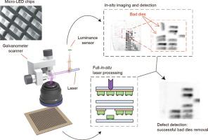
激光的非物理接触特性对精密工程中的对准过程提出了重大挑战。特别是在基于振镜的激光加工系统中,多步坐标转换的要求进一步使对准过程复杂化,从而增加了误差积累的可能性。为了解决振镜激光扫描过程中的对准问题,本文提出了一种全原位成像和激光处理系统的无对准误差解决方案,该方案通过跳过坐标转换,直接从捕获的图像中提取激光扫描的角坐标,消除了主级的对准误差。与现有的基于振镜的激光加工系统相比,该方法的主要优点是无需校准即可实现无校准误差,特别适合小批量、高度定制和复杂的加工任务。该系统特别便于在激光制造过程中进行在线检查、检测和测量。此外,在泛半导体制造中进行了两个实验案例,包括柔性印刷电路(FPC)切割和micro - led缺陷检测,以验证所提出的全原位处理系统的有效性。相应地,目前的实验比较突出了该系统的优势,同时实现了27 mm × 27 mm的最大范围和0.412µm的最小分辨率,最大处理误差为15µm。在检测和处理复杂图案的演示中说明了其在精密制造中无准直误差激光加工方面的卓越能力。
本文章由计算机程序翻译,如有差异,请以英文原文为准。

Galvanometer-Based Alignment-Error-Free Full-in-Situ Imaging and Laser Processing System with Applications to Pan-Semiconductor Manufacturing

Galvanometer-Based Alignment-Error-Free Full-in-Situ Imaging and Laser Processing System with Applications to Pan-Semiconductor Manufacturing
The non-physical-contact property of lasers poses significant challenges for the alignment procedure in precision engineering. Particularly in galvanometer-based laser processing systems, the requirement for multiple-step coordinate conversion further complicates the alignment procedure, thereby increasing the potential for error accumulation. To address the alignment issues during galvanometer laser scanning, this paper proposes an alignment-error-free solution for full-in-situ imaging and laser processing system, which eliminates the alignment error at the principal level by skipping the coordinate conversion and directly extracting angular coordinates for laser scanning from the captured images. Compared with the existing galvanometer-based laser processing systems, the main advantage of the proposed method is its ability to achieve alignment-error-free without requiring calibration, making it particularly suitable for small-batch, highly customized, and complex processing tasks. This system specifically facilitates in-line inspection, detection, and measurement during laser fabrications. Furthermore, two experimental cases in pan-semiconductor manufacturing, which includes flexible printed circuits (FPC) cutting and Micro-LEDs defect detection, have been conducted to demonstrate the validation of the proposed full-in-situ processing system. Correspondingly, the current experimental comparisons highlight the superiority of the proposed system for simultaneously achieving a maximum range of 27 mm × 27 mm and a minimum resolution of 0.412 µm, with a maximum processing error <15 µm. Demonstrations in detecting and processing the complex patterns illustrate its exceptional capabilities in alignment-error-free laser processing for precision manufacturing.
求助全文
通过发布文献求助,成功后即可免费获取论文全文。 去求助
来源期刊
Engineering
Engineering Environmental Science-Environmental Engineering
自引率
1.60%
发文量
335
审稿时长
35 days
期刊介绍: Engineering, an international open-access journal initiated by the Chinese Academy of Engineering (CAE) in 2015, serves as a distinguished platform for disseminating cutting-edge advancements in engineering R&D, sharing major research outputs, and highlighting key achievements worldwide. The journal's objectives encompass reporting progress in engineering science, fostering discussions on hot topics, addressing areas of interest, challenges, and prospects in engineering development, while considering human and environmental well-being and ethics in engineering. It aims to inspire breakthroughs and innovations with profound economic and social significance, propelling them to advanced international standards and transforming them into a new productive force. Ultimately, this endeavor seeks to bring about positive changes globally, benefit humanity, and shape a new future.
×
引用
GB/T 7714-2015
复制
MLA
复制
APA
复制
导出至
BibTeX EndNote RefMan NoteFirst NoteExpress
×
提示
您的信息不完整,为了账户安全,请先补充。
现在去补充
×
提示
您因"违规操作"
具体请查看互助需知
我知道了
×
提示
确定
请完成安全验证×
copy
已复制链接
快去分享给好友吧!
我知道了
右上角分享
点击右上角分享
0
联系我们:info@booksci.cn Book学术提供免费学术资源搜索服务,方便国内外学者检索中英文文献。致力于提供最便捷和优质的服务体验。 Copyright © 2023 布克学术 All rights reserved.
京ICP备2023020795号-1
ghs 京公网安备 11010802042870号
Book学术文献互助
Book学术文献互助群
群 号:604180095
Book学术官方微信