Ahmad Nizamuddin Muhammad Mustafa, Victoria Greenacre, Huanyu Zhou, Shibin Thomas, Tianyi Yin, Sarah Alodan, Yasir J. Noori, Giuseppe Mallia, Nicholas M. Harrison, Gillian Reid, Philip N. Bartlett, Kees de Groot, Sami Ramadan, Peter K. Petrov and Norbert Klein
{"title":"用于TMDC集成的硫退火石墨烯缺陷形成探测","authors":"Ahmad Nizamuddin Muhammad Mustafa, Victoria Greenacre, Huanyu Zhou, Shibin Thomas, Tianyi Yin, Sarah Alodan, Yasir J. Noori, Giuseppe Mallia, Nicholas M. Harrison, Gillian Reid, Philip N. Bartlett, Kees de Groot, Sami Ramadan, Peter K. Petrov and Norbert Klein","doi":"10.1039/D5NR01917F","DOIUrl":null,"url":null,"abstract":"<p >The integration of graphene with other 2D materials has been extensively studied over the past decade to realize high-performance devices unattainable with single materials. Graphene-transition metal dichalcogenides (TMDCs) such as MoS<small><sub>2</sub></small>, WS<small><sub>2</sub></small>, MoSe<small><sub>2</sub></small>, and WSe<small><sub>2</sub></small> vertical heterostructures have demonstrated promise in numerous electronic and optoelectronic applications due to the wide bandgap range and strong light–matter interaction in TMDCs, and the ability to form electrostatically tunable junctions with graphene. However, conventional methods for TMDCs growth, including chemical vapor deposition (CVD), electrodeposition, and atomic layer deposition (ALD), require high temperatures, which can degrade graphene's electrical and structural properties. Here, we investigate the impact of sulfur annealing on graphene, revealing significant etching and electrical degradation. Density functional theory (DFT) calculations identify the divacancy defect with two sulfur adatoms (DV-2S) and C–S–C bonds as the dominant defect, differing from the previously reported monovacancy with one sulfur adatom (MV-1S). This defect induces p-doping in graphene, consistent with experimental observations. To address these challenges, we introduce a protective strategy utilizing self-assembled monolayers (SAMs) during annealing, enabling the growth of high-quality WS<small><sub>2</sub></small> on graphene <em>via</em> electrodeposition. Our findings provide a foundation for integrating TMDCs with graphene while preserving its properties, advancing high-performance electronic and optoelectronic applications.</p>","PeriodicalId":92,"journal":{"name":"Nanoscale","volume":" 35","pages":" 20504-20518"},"PeriodicalIF":5.1000,"publicationDate":"2025-08-26","publicationTypes":"Journal Article","fieldsOfStudy":null,"isOpenAccess":false,"openAccessPdf":"https://pubs.rsc.org/en/content/articlepdf/2025/nr/d5nr01917f?page=search","citationCount":"0","resultStr":"{\"title\":\"Probing defect formation in sulfur-annealed graphene for TMDC integration\",\"authors\":\"Ahmad Nizamuddin Muhammad Mustafa, Victoria Greenacre, Huanyu Zhou, Shibin Thomas, Tianyi Yin, Sarah Alodan, Yasir J. Noori, Giuseppe Mallia, Nicholas M. Harrison, Gillian Reid, Philip N. Bartlett, Kees de Groot, Sami Ramadan, Peter K. Petrov and Norbert Klein\",\"doi\":\"10.1039/D5NR01917F\",\"DOIUrl\":null,\"url\":null,\"abstract\":\"<p >The integration of graphene with other 2D materials has been extensively studied over the past decade to realize high-performance devices unattainable with single materials. Graphene-transition metal dichalcogenides (TMDCs) such as MoS<small><sub>2</sub></small>, WS<small><sub>2</sub></small>, MoSe<small><sub>2</sub></small>, and WSe<small><sub>2</sub></small> vertical heterostructures have demonstrated promise in numerous electronic and optoelectronic applications due to the wide bandgap range and strong light–matter interaction in TMDCs, and the ability to form electrostatically tunable junctions with graphene. However, conventional methods for TMDCs growth, including chemical vapor deposition (CVD), electrodeposition, and atomic layer deposition (ALD), require high temperatures, which can degrade graphene's electrical and structural properties. Here, we investigate the impact of sulfur annealing on graphene, revealing significant etching and electrical degradation. Density functional theory (DFT) calculations identify the divacancy defect with two sulfur adatoms (DV-2S) and C–S–C bonds as the dominant defect, differing from the previously reported monovacancy with one sulfur adatom (MV-1S). This defect induces p-doping in graphene, consistent with experimental observations. To address these challenges, we introduce a protective strategy utilizing self-assembled monolayers (SAMs) during annealing, enabling the growth of high-quality WS<small><sub>2</sub></small> on graphene <em>via</em> electrodeposition. Our findings provide a foundation for integrating TMDCs with graphene while preserving its properties, advancing high-performance electronic and optoelectronic applications.</p>\",\"PeriodicalId\":92,\"journal\":{\"name\":\"Nanoscale\",\"volume\":\" 35\",\"pages\":\" 20504-20518\"},\"PeriodicalIF\":5.1000,\"publicationDate\":\"2025-08-26\",\"publicationTypes\":\"Journal Article\",\"fieldsOfStudy\":null,\"isOpenAccess\":false,\"openAccessPdf\":\"https://pubs.rsc.org/en/content/articlepdf/2025/nr/d5nr01917f?page=search\",\"citationCount\":\"0\",\"resultStr\":null,\"platform\":\"Semanticscholar\",\"paperid\":null,\"PeriodicalName\":\"Nanoscale\",\"FirstCategoryId\":\"88\",\"ListUrlMain\":\"https://pubs.rsc.org/en/content/articlelanding/2025/nr/d5nr01917f\",\"RegionNum\":3,\"RegionCategory\":\"材料科学\",\"ArticlePicture\":[],\"TitleCN\":null,\"AbstractTextCN\":null,\"PMCID\":null,\"EPubDate\":\"\",\"PubModel\":\"\",\"JCR\":\"Q1\",\"JCRName\":\"CHEMISTRY, MULTIDISCIPLINARY\",\"Score\":null,\"Total\":0}","platform":"Semanticscholar","paperid":null,"PeriodicalName":"Nanoscale","FirstCategoryId":"88","ListUrlMain":"https://pubs.rsc.org/en/content/articlelanding/2025/nr/d5nr01917f","RegionNum":3,"RegionCategory":"材料科学","ArticlePicture":[],"TitleCN":null,"AbstractTextCN":null,"PMCID":null,"EPubDate":"","PubModel":"","JCR":"Q1","JCRName":"CHEMISTRY, MULTIDISCIPLINARY","Score":null,"Total":0}
Probing defect formation in sulfur-annealed graphene for TMDC integration
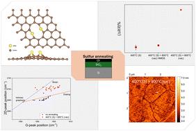
The integration of graphene with other 2D materials has been extensively studied over the past decade to realize high-performance devices unattainable with single materials. Graphene-transition metal dichalcogenides (TMDCs) such as MoS2, WS2, MoSe2, and WSe2 vertical heterostructures have demonstrated promise in numerous electronic and optoelectronic applications due to the wide bandgap range and strong light–matter interaction in TMDCs, and the ability to form electrostatically tunable junctions with graphene. However, conventional methods for TMDCs growth, including chemical vapor deposition (CVD), electrodeposition, and atomic layer deposition (ALD), require high temperatures, which can degrade graphene's electrical and structural properties. Here, we investigate the impact of sulfur annealing on graphene, revealing significant etching and electrical degradation. Density functional theory (DFT) calculations identify the divacancy defect with two sulfur adatoms (DV-2S) and C–S–C bonds as the dominant defect, differing from the previously reported monovacancy with one sulfur adatom (MV-1S). This defect induces p-doping in graphene, consistent with experimental observations. To address these challenges, we introduce a protective strategy utilizing self-assembled monolayers (SAMs) during annealing, enabling the growth of high-quality WS2 on graphene via electrodeposition. Our findings provide a foundation for integrating TMDCs with graphene while preserving its properties, advancing high-performance electronic and optoelectronic applications.
期刊介绍:
Nanoscale is a high-impact international journal, publishing high-quality research across nanoscience and nanotechnology. Nanoscale publishes a full mix of research articles on experimental and theoretical work, including reviews, communications, and full papers.Highly interdisciplinary, this journal appeals to scientists, researchers and professionals interested in nanoscience and nanotechnology, quantum materials and quantum technology, including the areas of physics, chemistry, biology, medicine, materials, energy/environment, information technology, detection science, healthcare and drug discovery, and electronics.


 求助内容:
求助内容: 应助结果提醒方式:


